
Part I The Lab Kit Manual
Chapter 1 Inventory
Each lab kit should contain the following items.
Section 1.1 Connectors
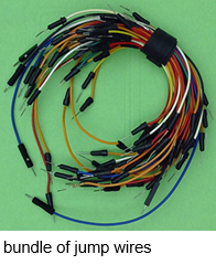
1 x bundle of jump wires
-
Used to connect the input and output terminals to the breadboard and different components on the breadboard to each other.
-
These jump wires come in four lengths about 12cm, 16cm, 20cm, & 24cm.
-
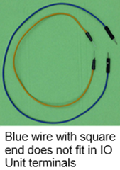
You may find some jump wires with square end terminals. You cannot use these in the U of L IO Unit’s terminals, but you can use them in the breadboard.
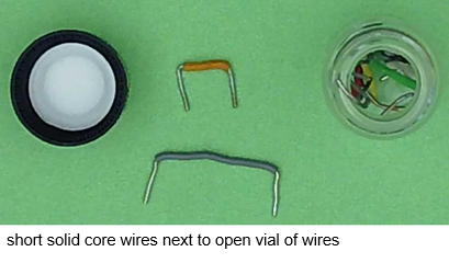
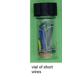
1 x vial of short solid core wires
-
To connect different components on the breadboard to each other.
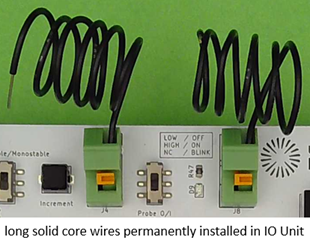
2 x long solid core wires
-
These wires stay inserted in the terminals at the top of the IO Unit.
-
The left wire is attached to the clock.
-
The right wire is attached to the probe.
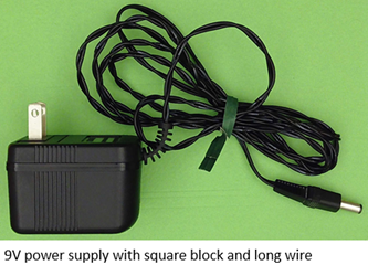
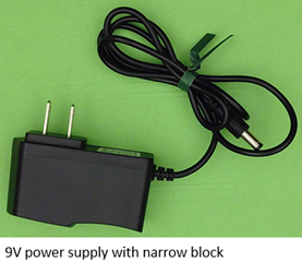
1 x 9V power supply
-
To connect the power in on the U of L IO Unit to a power socket.
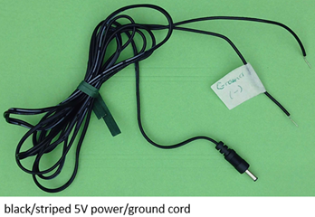
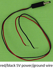
1 x 5V power/ground cord
-
To connect the power out on the U of L IO Unit to the breadboard.
-
The red or striped wire is connected to the power line (+).
-
The black or unstriped wire is connected to the ground line (-).
You have attempted of activities on this page.
Section 1.2 Tools
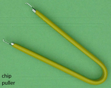
1 x chip puller
-
For removing chips from the breadboard.
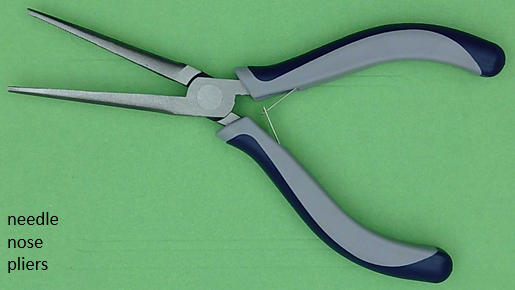
1 x needle nose pliers
-
For straightening the pins on chips.
You have attempted of activities on this page.
Section 1.3 Electronic parts
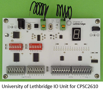
1 x U of L IO Unit
-
See the U of L IO Unit section.
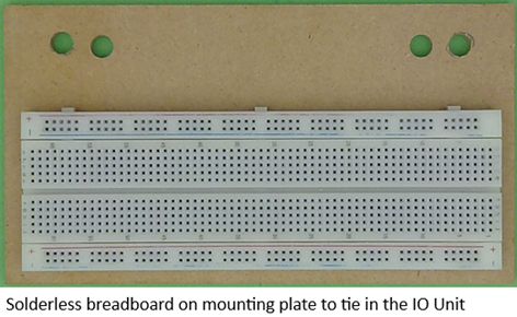
1 x breadboard
-
See the Breadboard section.
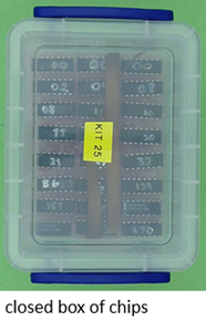
1 x plastic box of chips
-
The chips must be securely nestled in the antistatic foam, oriented correctly (with the notch on the left), and in chip number order from left to right then top to bottom.
-
See the ICs/Chips and 74LS* Reference sections.
You have attempted of activities on this page.
Chapter 2 Packing the Kit
Pack the box of chips and lab kit as follows.
Section 2.1 The Chip Set
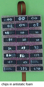
Chips in Antistatic Foam
-
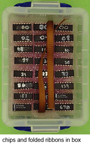
Place the chips in the antistatic foam which are oriented correctly (notch on the left), and in numerical order.
-
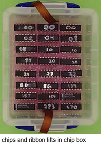
Put the foam with the chips in the chip box. Keep the ribbon lifts clear of the box.
-
Drape the ribbons ends over the chips.
-
Put the lid on the chip box and close the latches.
You have attempted of activities on this page.
Section 2.2 The Bottom Layer of the Lab Kit
-
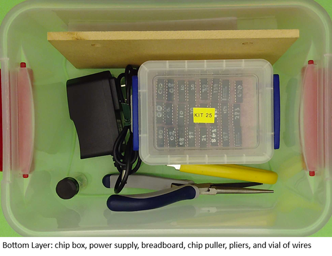
Place the box of chips in the bottom of the kit box with the kit label right way up.
-
Coil and fasten the cord of the power supply and place it in the kit to one side of the chip box.
-
Place the breadboard between the side of the kit box and the chip box.
-
Place the chip puller and needle nose pliers on the opposite side of the chip box between the side of the kit box and the chip box.
-
Place the vial of short wires in the corner of the kit box on the same side as the tools by the power supply.
You have attempted of activities on this page.
Section 2.3 The Middle Layer of the Lab Kit
-
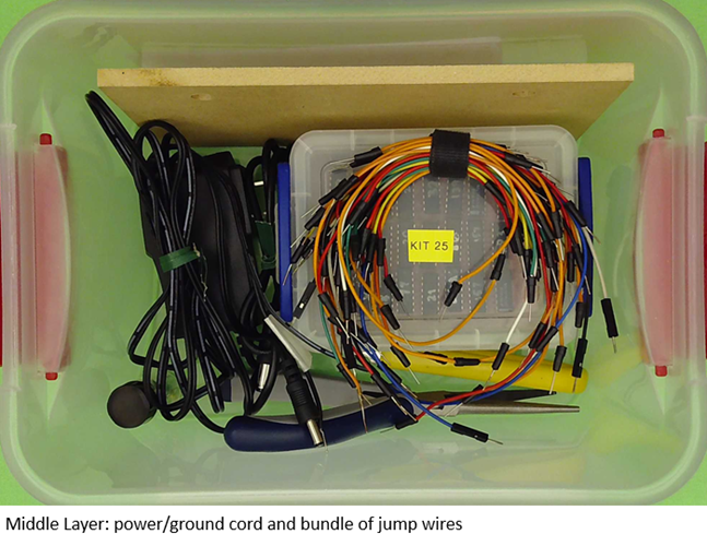
Coil and fasten the power/ground cord and place it on top of the power supply.
-
Fasten the jump wires with the velcro wrap to form a bundle.
-
Place the bundle of jump wires on top of the box of chips.
You have attempted of activities on this page.
Section 2.4 The Top Layer of the Lab Kit
-
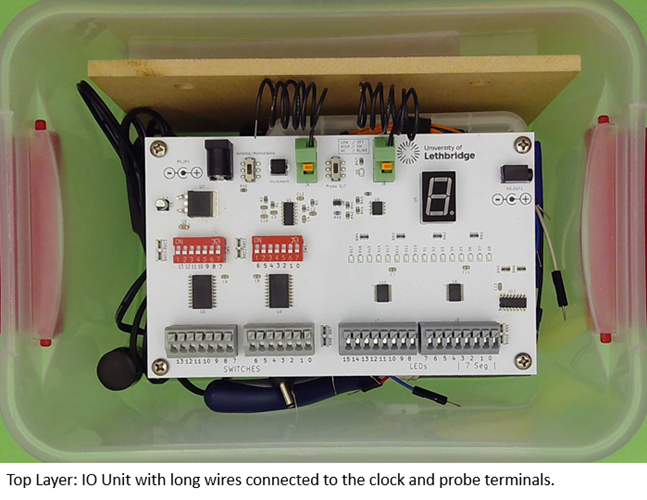
Set the U of L IO Unit on top of the power/ground cord and bundle of jump wires, face up, to prevent damage to the components.
-
Put the lid on the kit box and close the latches.
You have attempted of activities on this page.
Chapter 3 The University of Lethbridge IO Unit
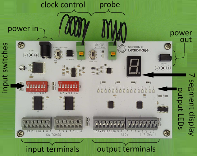
All the details about what the U of L IO Unit provides.
Section 3.1 General Notes
-
The U of L IO Unit provides:
-
Power and gounding for the breadboard
-
switches and a clock for input
-
LEDs and a seven segment display for output
-
a probe for troublshooting
-
-
For relative positions on the U of L IO Unit, like top, bottom, left and right:
-
Find the University of Lethbridge logo. Position the U of L IO Unit so the logo reads left to right and is the right way up.
-
This manual calls this standard orientation of the U of L IO Unit.
-
Descriptive locations on the board are always referred to with respect to this orientation.
-
You have attempted of activities on this page.
Section 3.2 Power
Subsection 3.2.1 Power in
-
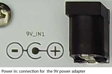
The power in port is in the upper left corner of the UofL IO Unit.
-
It is labelled 9V_In1.
-
Plug the 9-volt wall plug adapter in to a standard power socket and when you are ready to test your circuit plug the other end here.
Subsection 3.2.2 Power out
-
The power out port is in the upper right corner of the IO unit. It is labelled 5V_OUT1.
-
Plug the 5-volt power/ground cord here.
-
There are two types of The red wire or striped wire from this cable provides the 5-volts.
-
The black wire or unstriped wire (marked with tape) provides ground (0 volts).
-
This power cable is used to power and ground the breadboard.
-
You have attempted of activities on this page.
Section 3.3 Input
Subsection 3.3.1 Input Terminals & Switches
-
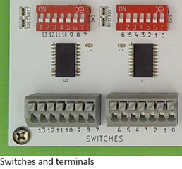
There are 14 input terminals and associated switches.
-
The input terminals are at the left side of the U of L IO Unit, at the bottom.
-
The input switches are at the left side of the U of L IO Unit, in the middle.
-
They are used to input data.
-
The numbers under the input terminals correspond to the black numbers under the switches printed on the U of L IO Unit’s circuit board.
-
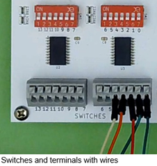
Jump wires with round end caps fit in the input terminals.
-
Press the button above a terminal to release the spring when putting a wire in or taking a wire out of the terminal.
-
The switches are slider swithces, on is marked on the switch panels.
-
Push the slider all the way to the top for on, 1, true, or closed.
-
Push the slider all the way to the bottom for off, 0, false, or open.
-
Subsection 3.3.2 Clock
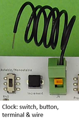
The clock controls and terminal are found at the top of the U of L IO Unit between the power-in port and the probe switch.
-
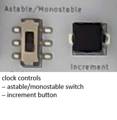
clock controls
-
astable/monostable switch
-
astable (up): the clock runs automatically
-
monostable (down): the clock is controlled by the increment button
-
-
increment button
-
push down: for the positive edge of the clock from 0 to 1 or off to on
-
release: for the negative edge of the clock from 1 to 0 or on to off
-
-
-
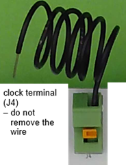
clock terminal
-
The clock terminal is labelled J4 on the U of L IO Unit.
-
a long solid core wire is connected at this terminal
-
attach this wire to the breadboard to use the clock you can test the clock by attaching this wire to an output terminal
-
do not remove this wire
-
You have attempted of activities on this page.
Section 3.4 Output
Subsection 3.4.1 Output Terminals & LEDs
-
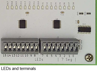
There are 16 output terminals and associated LEDs.
-
The output terminals are at the right side of the U of L IO Unit, at the bottom.
-
The associated LEDs are on the right side of the U of L IO Unit, in the middle.
-
They are used to output data.
-
The numbers under the output terminals, 0, 1, 2, ..., 15 correspond to the LEDs labelled D8, D7, ...D1, D10, D11, ... D17.
-
Jump wires with round end caps fit in the output terminals.
-
Press the button above a terminal to release the spring when putting a wire in or taking a wire out of the terminal.
-
An LED that is powered indicates on, 1, true, or high.
-
An LED that is not powered indicates off, 0, false, or low.
-
Subsection 3.4.2 Output Terminals & the Seven Segment Display
-
Output terminals 0, 1, 2, & 3 are connected to LEDs D8, D7, D6, & D5 and the 7-segment display.
-
The 7-segment display has 16 different states that correspond to the binary representation of the values from 0000 to 1111 and the hexidecimal values from 0 to F shown on the LEDs.
-
Unfortunately, this unit doesn’t show the letters A to F.The table below shows the 16 states and the values they represent.

Note: the display is blank when the output value is \(1111_2 = 15_10 = F_16\text{.}\)
Subsection 3.4.3 Probe
-
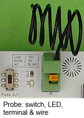
The probe allows you to observe signals within your design and is helpful for debugging.
-
The probe is in the middle of the top edge of the IO unit, next to the clock.
-
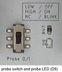
The probe slider switch turns the probe on or off.
-
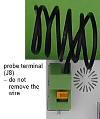
A long wire is connected to the probe’s terminal. Do not remove this wire from the terminal.
-
The probe has a three state LED.
-
If the probe wire is touching to a grounded connection (turned off/set to low/set to 0) then the light will be off.
-
If the probe wire is touching a powered connection (turned on/set to high/set to 1) then the light will be on.
-
If the probe wire is touching nothing or touching a connection that is neither powered nor grounded then it will blink.
-
Touch the probe wire to chip pins to determine the state of inputs and outputs.
-
Use the information to identify errors, broken wires, and malfunctioning chips.
-
You have attempted of activities on this page.
Chapter 4 The Breadboard
The solderless breadboard is the part of your kit used to connect chips to each other and to the U of L IO Unit.
Section 4.1 Description
-
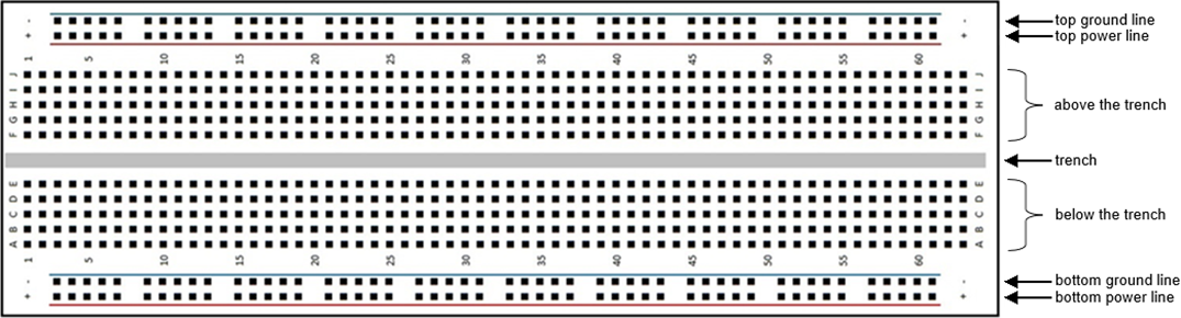
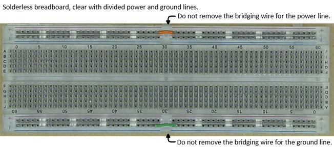
power and ground lines:
-
A conductive metal strip is positioned horizontally under each power and ground line.
-
If you have one of the new clear breadboards with the divided power and ground line then a short wire has been inserted to bridge the gap in the power and ground lines. Do not remove the bridging wires from the breadboard.
-
-
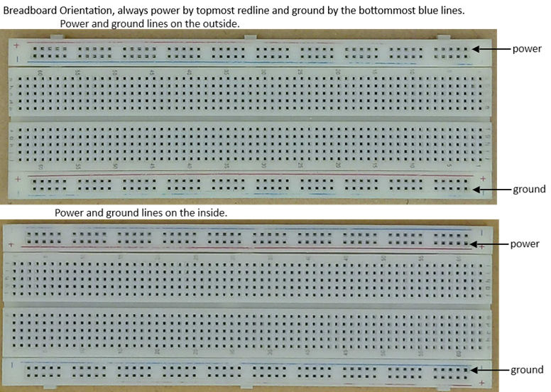
The ground line may be above the power line or the power line may be above the ground line.
-
Put the power wire of the power/ground cord in a hole at the right end of the top power line, the one next to the red line.
-
Put the ground wire of the power/ground cord in a hole at the right end of the bottom ground line, the one next to the blue line.
-
-
Conductive metal strips are positioned vertically under each column of holes above the trench and each column of holes below the strip.
-
Each of the holes the above and below the trench can be identified by row letter and column number.
-
The conductive metal strips do not cross the trench, so holes on opposite side of the trench are not connected.
-
You have attempted of activities on this page.
Section 4.2 Use
-
All chips must straddle the gutter down the center of the bread board, that is, half the leads will be in row E and the other half in row F.
-
The integrated circuits in your lab kit can be damaged if you switch their connections to power and ground. Therefore, we will reserve two colours of lines to help prevent this from happening.
-
The top most red line is always (and only) connected to power (the red or striped wire of the power/ground cord).
-
The bottom most blue line is always (and only) connected to ground (the black or plain and labelled wire of the power/ground cord).
-
You have attempted of activities on this page.
Chapter 5 Integrated Circuits or ICs
Section 5.1 Description
-
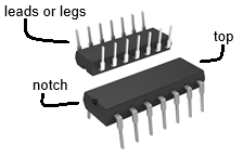
The chips in your kit come from a standardized selection of logic parts known as the 7400 (said “seventy-four hundred”) series.
-
The form of each part number is MM74FFNNP where:
-
MM is a code that identifies the company that manufactured the chip.
-
FF indicates the family of chips this part belongs to, in our case LS or “Advanced Low-power Schottky”) parts.
-
NN indicates the logical function of the part (see 74LS* Reference).
-
P is the kind of packaging used. The parts in our kit usually have “N” (for plastic, dual-inline).
-
You have attempted of activities on this page.
Section 5.2 Orientation
-
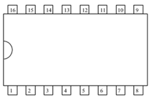
A small notch is carved in one end of a chip to designate pin numbering, and pins are numbered counterclockwise from pin 1.
-
Chips should be plugged into the board straddling the trench with the notch on the left and pin 1 in the lower left corner.
You have attempted of activities on this page.
Section 5.3 Insertion
-
You should unplug the U of L IO Unit before you insert an IC.
-
Use uniform pressure across the top of the IC when inserting it into the breadboard:
-
This will prevent the pins from bending.
-
You may have to use the needle nose pliers adjust the distance between the two rows of pins before insertion.
-
-
Leave at least three rows of empty holes between chips so that the chip puller can fit around the chip.
You have attempted of activities on this page.
Section 5.4 Removal
-
You should unplug the U of L IO Unit before you remove an IC. Always use a chip puller when removing chips from a breadboard or a socket on a printed circuit board.
-
To use a chip puller:
-
Place the jaws of the chip puller against the trench on either side of the chip.
-
Squeeze the jaws of the chip puller until they are over the ends of the chip and the chip haas popped out of the breadboard.
-
Pull straight up, evenly, to protect the pins.
-
You have attempted of activities on this page.
Chapter 6 74LS* Reference
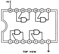
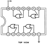
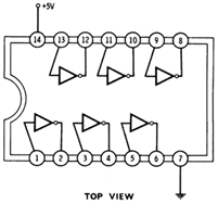
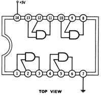
For all the chips in this kit the ground is the rightmost of the pins at the bottom and the power is the leftmost of the pins at the top. The quantity of chips of each type in the kit is listed after the chip’s name in parentheses.
Section 6.1 Chips with Basic Logic Gates
Subsection 6.1.1 74LS00 Quad 2-Input NAND gates (3)
-
All four NAND gates may be used independently.
-
On any one gate, when either input is low the output is driven high.
-
If both inputs are high the output is low.
Subsection 6.1.2 74LS02 Quad 2-Input NOR gates (1)
-
All four NOR gates may be used independently.
-
On any one gate, with either input high the output is low.
-
When both inputs are low the output is high.
-
Note: on this chip the gates are backward relative to the other gate chips.
Subsection 6.1.3 74LS04 Hex Inverter (1)
-
All six inverters may be used independently.
-
On any one inverter, the low-input condition drives the output high.
-
The high-input condition drives the output low.
Subsection 6.1.4 74LS08 Quad 2-Input AND gates (2)
-
All four AND gates may be used independently.
-
On any one gate, when either input is low, the output is low.
-
When both inputs are high the output is high
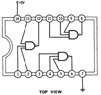
Subsection 6.1.5 74LS10 Triple 3-Input NAND gates (2)
-
All three NAND gates may be used independently.
-
On any one gate, when any input is low, the output is driven to a high state.
-
When all three inputs are high, the output is driven to a low state
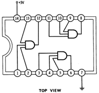
Subsection 6.1.6 74LS11 Triple 3-Input AND gates (1)
-
All three AND gates may be used independently.
-
On any one gate, when any input is low, the output is driven to a low state.
-
When all three inputs are high, the output is driven to a high state.
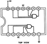
Subsection 6.1.7 74LS20 Dual 4-Input NAND gates (2)
-
Both 4-input gates may be used independently.
-
On either gate, any input-low condition drives the out- put high.
-
When all inputs are high, the output is low.
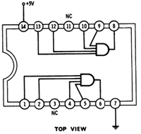
Subsection 6.1.8 74LS21 Dual 4-Input AND gates (1)
-
Both 4-input gates may be used independently.
-
On either gate, any input-low condition drives the out- put low.
-
When all inputs are high, the output is high.
Subsection 6.1.9 74LS27 Triple 3-Input NOR gates (1)
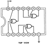
-
All three NOR gates may be used independently.
-
On any one gate, when any input is high, the output is driven to a low state.
-
When all three inputs are low, the output is driven to a high state
Subsection 6.1.10 74LS32 Quad 2-Input OR gates (1)
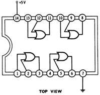
-
All four OR gates may be used independently.
-
On any one gate, when either input is high, the output is driven high.
-
When both inputs are low the output is low.
Subsection 6.1.11 74LS86 Quad Exclusive-OR gates (2)
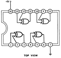
-
All four XOR gates may be used independently.
-
On any one gate, when one, but not both, inputs are high, the output is high.
-
When both inputs are high or both inputs are low, the output is low.
You have attempted of activities on this page.
Section 6.2 Chips with complex functions
Subsection 6.2.1 74LS139 Dual 2→4 Decoder (1)
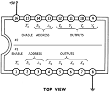
-
The chip contains two individual decoders.
-
Each decoder drives one line according to the binary value at its address.
-
This circuit can also be used to make a 3→8 decoder.
-
Suppose we have inputs \(I\text{,}\) \(J\text{,}\) and \(K\text{.}\)
-
Connect \(I\) to \(\overline{E_1}\) and connect \(I\) to \(\overline{E_2}\) using an inverter.
-
Connect \(J\) to both \(A_1\) and \(A_2\text{.}\)
-
Connect \(K\) to both \(B_1\) and \(B_2\text{.}\)
-
| Enable | \(A_iB_i\) | \(X_0/Y_0\) | \(X_1/Y_1\) | \(X_2/Y_2\) | \(X_3/Y_3\) |
| 0 | 00 | 0 | 1 | 1 | 1 |
| 0 | 00 | 1 | 0 | 1 | 1 |
| 0 | 00 | 1 | 1 | 0 | 1 |
| 0 | 00 | 1 | 1 | 1 | 0 |
| 1 | XX | 1 | 1 | 1 | 1 |
Subsection 6.2.2 74LS157 Quad 1-of-2 Multiplexer (2)
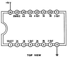
-
This device selects (SELECT) between two inputs (A and B) to drive the output (OUT).
-
All four of the switches are simultaneously enabled or selected.
-
If the Enable input is high, all outputs will be low.
-
Otherwise, the Select determines whether the A or B inputs control the output.
Subsection 6.2.3 74LS175 Quad "D" Memory (2)
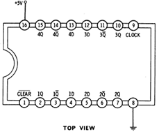
-
Four bits of memory are stored in four separate positive-edge triggered D-type flip-flops, each with normal, Q, and complementary, Q, output.
-
Information at the D inputs is entered in all 4 bits of memory simultaneously on the positive edge of the clock.
-
The Clear input is normally held high, bringing it to ground will clear the memory, making all Q outputs low.
Subsection 6.2.4 74LS283 4-Bit Full Adder (1)
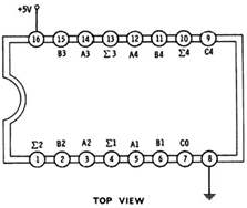
-
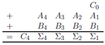
This is an arithmetic unit that provides the sum of two 4-bit binary numbers and an input carry C0 as follows:
Subsection 6.2.5 74LS670 4x4 Register File (1)
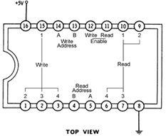
-
The register file is organized as four 4-bit locations.
-
The independent \(\overline{\text{Enable}}\) and addresses for read and write permits simultaneous writing into one location and reading from another location.
-
The outputs are Read 1, 2, 3, 4.
-
The inputs are Write 1, 2, 3, 4; Read Address AB; Write Address AB; Write \(\overline{\text{Enable}}\text{;}\) and Read \(\overline{\text{Enable}}\text{.}\)
-
To save 1101 to memory location 2
-
Set the write \(\overline{\text{Enable}}\) to 1, the read \(\overline{\text{Enable}}\) to 0.
-
Set the read and write addresses AB=10.
-
Set Write 1, 2, 3, 4 to 1101.
-
Change the write \(\overline{\text{Enable}}\) to 0, pause, then set it to 0.
-
To read memory location 1
-
Set the write \(\overline{\text{Enable}}\) to 1, the read \(\overline{\text{Enable}}\) to 0.
-
Set the read addresses AB=01.
-
The contents of the memory will be displayed by Read 1, 2, 3, 4.
You have attempted of activities on this page.