Part II Lab Material

Chapter 7 Boolean Operators, Gates, and Chips

Section 7.1 Negation/Not, \(A'\)

  • Negation/not is a unary operator.
  • The symbol for negation/not is \('\text{,}\) it appears after the operand/variable.
    • A bar over a variable or expression is sometimes used to indicate negation/not, \(\overline{A}\text{.}\) We favour the single quote because it is easier to type.
  • When a statment is negated a result/output of 0 becomes 1 and a result/output of 1 becomes 0.
  • The gate for negation/not is called an inverter gate.
\(A\) \(A'\)
0 1
1 0
inverter gate
inverter gate
You have attempted of activities on this page.

Section 7.2 OR, \(A + B\)

  • The symbol used for OR is \(+\text{.}\)
  • OROR is a binary operator but more than two variables/expressions can be strung together with or to form an or statement.
  • An or statement only results in a 0 if all operands are 0.
\(A\) \(B\) \(A + B\)
0 0 0
0 1 1
1 0 1
1 1 1
OR gates
2 input OR gate
You have attempted of activities on this page.

Section 7.3 AND, \(A \cdot B\) or \(AB\)

  • The symbol used for AND is \(\cdot\text{,}\) or no symbol (called adjacency).
  • AND is a binary operator but more than two variables/expressions can be strung together with and to form an and statement.
  • An and statement only results in a 1 if all operands are 1.
\(A\) \(B\) \(A \cdot B\)
0 0 0
0 1 0
1 0 0
1 1 1
AND gates
2 input AND gate
3 input AND gate
4 input AND gate
You have attempted of activities on this page.

Section 7.4 XOR, \(A \oplus B\)

\(A\) \(B\) \(A \oplus B\)
0 0 0
0 1 1
1 0 1
1 1 0
2 input XOR gates
2 input XOR gate
You have attempted of activities on this page.

Section 7.5 NOR, \((A + B)'\)

  • NOR is the negation of OR.
  • There is no standard single symbol for NOR, but we sometimes write \(A \text{NOR} B\text{.}\)
  • NOR is a binary operator but more than two variables/expressions can be strung together with nor to form an nor statement.
  • A nor statement only results in a 1 if all operands are 0.
\(A\) \(B\) \((A + B)'\)
0 0 1
0 1 0
1 0 0
1 1 0
NOR gates
2 input NOR gate
3 input NOR gate
You have attempted of activities on this page.

Section 7.6 NAND, \((A \cdot B)'\) / \((AB)'\)

  • NAND is the negation of AND.
  • There is no standard single symbol for NAND, but we sometimes write \(A \text{NAND} B\text{.}\)
  • NAND is a binary operator but more than two variables/expressions can be strung together with nand to form a nand statement.
  • An nand statement only results in a 0 if all operands are 1.
\(A\) \(B\) \((A \cdot B)'\)
0 0 1
0 1 1
1 0 1
1 1 0
NAND gates
2 input NAND gate
3 input NAND gate
4 input NAND gate
You have attempted of activities on this page.

Chapter 8 How to set up a truth table

A truth table shows all the possible combination of values for the input operands/variables and the value of each output result/variable in each case.

Section 8.1 The input side of the truth table

  • A truth table is a special table of values for boolean expressions and circuits.
  • In the labs for this course, all truth tables will have the following format:
  • For a truth table with \(n\) input operands/columns...
    • The table will have \(2^n\) rows.
    • The input columns will contain all the possible combinations of binary values with \(n\) digits in ascending numerical order.
    • An easy way to set up the input columns:
      1. In the first input column set the top half of the column to \(0\) and the bottom half to \(1\text{.}\)
      2. For each subsequent column β€œhalve the pattern." That is if you set \(a\) of the entries in the previous column to \(0\) then set the first \(\frac{a}{2}\) of the entries to \(0\text{,}\) the next \(\frac{a}{2}\) entries to \(1\) and repeat until you reach the bottom of the column.
      3. The last column should always contain alternating \(0\) s and \(1\) s.
    • All the remaining columns are output columns which indicate the result of evaluating a boolean expression with the given inputs, or the output for a circuit when the switches are set to the given inputs.

Example 8.1.1. Set up a truth table.

  • Suppose we wanted to make a truth table for \(x = (A' \oplus B) \cdot C\) and \(y = (B' \cdot C)' + D\text{.}\)
  • There are four input operands, \(A\text{,}\) \(B\text{,}\) \(C\text{,}\) and \(D\text{.}\) So, the table will need four input columns, hence \(n = 4\text{.}\)
  • The table will have \(2^n = 2^4 = 16\) rows.
    • Start the pattern: The first input column will have \(\frac{16}{2} = 8\) zeros then \(8\) ones.
    • Half the pattern: The second input column will have \(\frac{8}{2} = 4\) zeros then \(4\) ones in a repeating pattern.
    • Half the pattern: The third input column will have \(\frac{4}{2} = 2\) zeros then \(2\) ones in a repeating pattern.
    • Half the pattern: The fourth input column will have \(\frac{2}{2} = 1\) zero then \(1\) one in an alternating pattern. Since there are alternating zeros and ones we know this is the last input column.
Table 8.1.2. Truth table for four operands
\(A\) \(B\) \(C\) \(D\) \(X\) \(Y\)
0 0 0 0
0 0 0 1
0 0 1 0
0 0 1 1
0 1 0 0
0 1 0 1
0 1 1 0
0 1 1 1
1 0 0 0
1 0 0 1
1 0 1 0
1 0 1 1
1 1 0 0
1 1 0 1
1 1 1 0
1 1 1 1
You have attempted of activities on this page.

Chapter 9 Boolean Algebra

Section 9.1 Basic Laws, Rules, Theorems and Properties of Boolean Algebra

Identity rule
\(x + 0 = x\)
\(x \cdot 1 = x\)
Null rule
\(x + 1 = 1\)
\(x \cdot 0 = 0\)
Inverse theorem
\(x + x' = 1\)
\(x \cdot x' = 0\)
Idempotent theorem
\(x + x = x\)
\(x \cdot x = x\)
Commutative theorem
\(x + y = y + x\)
\(x \cdot y = y \cdot x\)
Associative theorem
\((x + y) + z = x + (y + z)\)
\((x \cdot y) \cdot z = x \cdot (y \cdot z)\)
Absorbtion theorem
\(x + xy = x\)
\(x \cdot (x + y) = x\)
Involution theorem
\((x')' = x\)
\(\)
DeMorgan’s law
\((x + y)' = x' \cdot y'\)
\((x \cdot y)' = x' + y'\)
Distributive law
\(x \cdot (y + z) = x \cdot y + x \cdot z\)
\(x + (y \cdot z) = (x + y) \cdot (x + z)\)
You have attempted of activities on this page.

Section 9.2 Properties related to xor

Expanding rule
\(x \oplus y = (x + y) \cdot (x' + y') = (x \cdot y') + (x' \cdot y)\)
Negation rule
\((x \oplus y)' = (x' \oplus y) = (x \oplus y')\)
Hence...
\(x' \oplus y' = (x \oplus y')' = ((x \oplus y)')' = x \oplus y\)
You have attempted of activities on this page.

Chapter 10 SOP algorithm and Min Terms

Section 10.1 Sum of Products Algorithm

The Sum of Products algorithm (SOP) is a method for finding a boolean expression that corresponds to a given truth table.
  1. For each row of the output column that has a value of 1 create a product as follows:
    1. Make a boolean expression using all the input variables connected by AND operators.
    2. For each input variable that has a value of 0 in this column, negate that variable in the expression.
  2. Form a boolean expression by connecting all the products with OR operators. This is the sum of the products.

Example 10.1.1. Use the Sum of Products Algorithm.

Make a product for each row in the \(F\) column that has a value of 1.
Table 10.1.2. Truth Table
Row \(a\) \(b\) \(c\) \(F\) Product
0 0 0 0 0
1 0 0 1 0
2 0 1 0 1 \(A' \cdot B \cdot C'\)
3 0 1 1 0
4 1 0 0 1 \(A \cdot B' \cdot C'\)
5 1 0 1 0
6 1 1 0 1 \(A \cdot B \cdot C'\)
7 1 1 1 1 \(A \cdot B \cdot C\)
Make the sum by connecting all the products with OR operators.
\(F = (A' \cdot B \cdot C') + (A \cdot B' \cdot C') + (A \cdot B \cdot C') + (A \cdot B \cdot C)\)
You have attempted of activities on this page.

Section 10.2 Min Terms

Min Terms are all the products found using SOP expressed as the decimal value that corresponds to the inputs or if you set up the truth tables the way we do in this class, the value is the row number.
The values are usually given as a set in the following format \(G(x, y, z) = \Sigma(3, 5, 7)\)

Example 10.2.1. Find the max terms.

Note the rows that have an output of 1
Table 10.2.2. Truth Table
Row \(A\) \(B\) \(C\) \(F\)
0 0 0 0 0
1 0 0 1 0
2 0 1 0 1
3 0 1 1 0
4 1 0 0 1
5 1 0 1 0
6 1 1 0 1
7 1 1 1 1
Notice that the row numbers are the decimal value of the three bit number \(ABC\text{.}\)
ie: For row 3, \(ABC = 011\) and \(011_2 = 3_{10}\text{.}\)
So, the minterms for \(F\) are written \(F(A, B, C) = \Sigma (2, 4, 6, 7)\)
You have attempted of activities on this page.

Chapter 11 POS algorithm and Max Terms

Section 11.1 Sum of Products Algorithm

The Product of Sums algorithm (POS) is a method for finding a boolean expression that corresponds to a given truth table.
  1. For each row of the output column that has a value of 0 create a sum as follows:
    1. Make a boolean expression using all the input variables connected by OR operators.
    2. For each input variable that has a value of 1 in this column, negate that variable in the expression.
  2. Form a boolean expression by connecting all the sums with AND operators. This is the product of the sums.

Example 11.1.1. Use the Product of Sums Algorithm.

Make a sum for each row in the \(F\) column that has a value of 0.
Table 11.1.2. Truth Table
Row \(a\) \(b\) \(c\) \(F\) Product
0 0 0 0 0 \(A + B + C\)
1 0 0 1 0 \(A+B+C'\)
2 0 1 0 1
3 0 1 1 0 \(A+B'+C'\)
4 1 0 0 1
5 1 0 1 0 \(A'+B+C'\)
6 1 1 0 1
7 1 1 1 1
Make the product by connecting all the sums with AND operators.
\(F = (A+B+C) \cdot (A+B+C') \cdot (A+B'+C') \cdot (A'+B+C')\)
You have attempted of activities on this page.

Section 11.2 Max Terms

Max Terms are all the sums found using POS expressed as the decimal value that corresponds to the inputs or if you set up the truth tables the way we do in this class, the value is the row number.
The values are usually given as a set in the following format \(G(x, y, z) = \Pi(0, 1, 2, 4, 6)\)

Example 11.2.1. Find the max terms.

Note the rows that have an output of 1
Table 11.2.2. Truth Table
Row \(A\) \(B\) \(C\) \(F\)
0 0 0 0 0
1 0 0 1 0
2 0 1 0 1
3 0 1 1 0
4 1 0 0 1
5 1 0 1 0
6 1 1 0 1
7 1 1 1 1
Notice that the row numbers are the decimal value of the three bit number \(ABC\text{.}\)
ie: For row 5, \(ABC = 101\) and \(101_2 = 5_{10}\text{.}\)
So, the maxterms for \(F\) are written \(F(A, B, C) = \Pi (0, 1, 3, 5)\)
You have attempted of activities on this page.

Chapter 12 Don’t Cares

A don’t care is an output that indicates this set of input values will not be used, or this result doesn’t matter, or the result is neither 0 nor 1.

Section 12.1 How to use a don’t care

To indicate a don’t care in a truth table enter either \(x\text{,}\) \(X\text{,}\) or \(\phi\text{.}\)
For SOP and ignore a don’t care.
For minterms or maxterms indicate the don’t cares in their own set.

Example 12.1.1. Don’t care in a truth table.

Table 12.1.2. Codes for shopping order states: Pending, Shipped, and Delivered.
Row \(c_1\) \(c_2\) \(P\) \(S\) \(D\)
\(0\) \(0\) \(0\) \(1\) \(0\) \(0\)
\(1\) \(0\) \(1\) \(0\) \(1\) \(0\)
\(2\) \(1\) \(0\) \(0\) \(0\) \(1\)
\(3\) \(1\) \(1\) \(x\) \(x\) \(x\)
SOP:
Max terms:
POS:
Min terms:
You have attempted of activities on this page.

Chapter 13 Karnaugh map (K-map)

A Karnaugh map or K-map is a method for creating simplified boolean expressions from the set of all truth values which might be expressed as a truth table, minterms, or maxterms.

Section 13.1 How to make a K-map

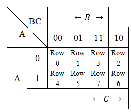
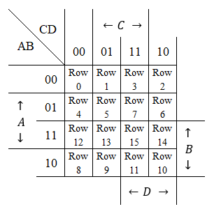
A K-map arranges the truth values in a grid so that adjacent values correspond to input values that differ by only one bit.
A K-map for three variables, say \(A\text{,}\) \(B\text{,}\) and \(C\text{,}\) the grid is two by four and is filled in this manner.
K-map info for 3 input variables
A K-map for three variables, say \(A\text{,}\) \(B\text{,}\) \(C\text{,}\) and \(D\) the grid is four by four and is filled in this manner.
K-map info for 4 input variables

Example 13.1.1. Make K-map from a min terms with three variables.

Make a k-map for \(F_1(A, B, C) = \Sigma (0, 3, 4, 6)\text{.}\)
Table 13.1.2. K-map for \(F_1(A, B, C)\)
\(F_1\) \(BC\) \(B'\) \(B'\) \(B\) \(B\)
\(A\) \(00\) \(01\) \(11\) \(10\)
\(A'\) \(0\) \(1_{r_{0}}\) \(0\) \(1_{r_{3}}\) \(0\)
\(A\) \(1\) \(1_{r_{4}}\) \(0\) \(0\) \(1_{r_{6}}\)
\(C'\) \(C\) \(C\) \(C'\)

Example 13.1.3. Make K-map from a min terms with four variables.

Make a K-map for \(F_2(A, B, C, D) = \Sigma (1, 3, 4, 6, 7, 9, 11, 12, 14, 15)\text{.}\)
Table 13.1.4. K-map for \(F_2(A, B, C, D)\)
\(F_2\) \(CD\) \(C'\) \(C'\) \(C\) \(C\) \(\)
\(AB\) \(00\) \(01\) \(11\) \(10\)
\(A'\) \(00\) \(0\) \(1_{r_{1}}\) \(1_{r_{3}}\) \(0\) \(B'\)
\(A'\) \(01\) \(1_{r_{4}}\) \(0\) \(1_{r_{7}}\) \(1_{r_{6}}\) \(B\)
\(A\) \(11\) \(1_{r_{12}}\) \(0\) \(1_{r_{15}}\) \(1_{r_{14}}\) \(B\)
\(A\) \(10\) \(0\) \(1_{r_{9}}\) \(1_{r_{11}}\) \(0\) \(B'\)
\(D'\) \(D\) \(D\) \(D'\)
You have attempted of activities on this page.

Section 13.2 How to use a K-map

  • Circling adjacent squares that contain ones.
    • Use the largest circles with dimensions that are powers of two. ie: 1x1, 1x2, 2x1, 2x2, 2x4, 4x2, etc.
    • Circles can wrap around the edge of the map to the opposite side.
    • It is better to circle a one more than once rather than use smaller circles.
  • Form boolean expressions, called prime implicants.
    • Examine all the entries/squares in each circle and determine the boolean variable and/or negated boolean variables they all have in common.
    • Put the list of variables and negated variables together with AND operators.
  • Your final expression may only contain the essential prime implicants.
    • Every prime implicant in the set of essential prime implicants contains at least one 1 that is only found in this prime implicant. In other words, remove any prime implicants that are not needed to obtain the original set of truth values. Recall: always favour a prime implicant that covers more ones over one that covers fewer.
    • Sometimes there is more than one way to form a set of essential prime implicants.
  • The boolean expression is formed by connecting all the essential prime implicants with OR operators.

Example 13.2.1. Use a k-map to find a boolean expression for \(F_3(A, B, C)\).

Table 13.2.2. K-map for \(F_3(A, B, C) = \Sigma (0, 3, 4, 6), d = \Sigma (5)\)
\(F_3\) \(BC\) \(B'\) \(B'\) \(B\) \(B\)
\(A\) \(00\) \(01\) \(11\) \(10\)
\(A'\) \(0\) \(1_{r_{0}}\) \(0\) \(1_{r_{3}}\) \(0\)
\(A\) \(1\) \(1_{r_{4}}\) \(X_{r_{5}}\) \(0\) \(1_{r_{6}}\)
\(C'\) \(C\) \(C\) \(C'\)
  • The largest circles that encompass all the ones and may encompass the don’t cares are:
    • \(\{ r_0, r_4 \}\text{,}\) \(\{ r_4, r_6 \}\text{,}\) and \(\{ r_3 \}\text{.}\)
  • Determine the variables in common for each circle/group:
    • \(\{ r_0,r_4 \}\) are in a column labelled \(B'\) and \(C'\text{,}\) so the prime implicant is \(B'C'\text{.}\)
    • \(\{ r_4, r_6 \}\) are in a row labelled \(A\) and columns both labelled \(C'\text{,}\) so the prime implicant is \(AC'\text{.}\)
    • \(\{ r_3 \}\) are in the row labelled \(A'\) and a column labelled \(B\) and \(C\text{,}\) so the prime implicant is \(A'BC\text{.}\)
  • Hence, the boolean expression found using the k-map is
    \begin{equation*} F_3(A,B,C) = B'C' + AC' + A'BC\text{.} \end{equation*}

Example 13.2.3. Use a k-map to find a boolean expression for \(F_3(A, B, C)\).

Table 13.2.4. K-map for \(F_3(A, B, C) = \Sigma (0, 3, 4, 6), d = \Sigma (5)\)
\(F_3\) \(BC\) \(B'\) \(B'\) \(B\) \(B\)
\(A\) \(00\) \(01\) \(11\) \(10\)
\(A'\) \(0\) \(1_{r_{0}}\) \(0\) \(1_{r_{3}}\) \(0\)
\(A\) \(1\) \(1_{r_{4}}\) \(X_{r_{5}}\) \(0\) \(1_{r_{6}}\)
\(C'\) \(C\) \(C\) \(C'\)
  • The largest circles that encompass all the ones and may encompass the don’t cares are:
    • \(\{ r_0, r_4 \}\text{,}\) \(\{ r_4, r_6 \}\text{,}\) and \(\{ r_3 \}\text{.}\)
  • Determine the variables in common for each circle/group:
    • \(\{ r_0,r_4 \}\) are in a column labelled \(B'\) and \(C'\text{,}\) so the prime implicant is \(B'C'\text{.}\)
    • \(\{ r_4, r_6 \}\) are in a row labelled \(A\) and columns both labelled \(C'\text{,}\) so the prime implicant is \(AC'\text{.}\)
    • \(\{ r_3 \}\) are in the row labelled \(A'\) and a column labelled \(B\) and \(C\text{,}\) so the prime implicant is \(A'BC\text{.}\)
  • Hence, the boolean expression found using the k-map is
    \begin{equation*} F_3(A,B,C) = B'C' + AC' + A'BC\text{.} \end{equation*}

Example 13.2.5. Use a k-map to find a boolean expression for \(F_4(A, B, C, D)\).

Table 13.2.6. K-map for \(F_4(A, B, C, D) = \Sigma (1, 3, 4, 6, 7, 11, 12, 14, 15), d = \Sigma (9, 13)\)
\(F_4\) \(CD\) \(C'\) \(C'\) \(C\) \(C\) \(\)
\(AB\) \(00\) \(01\) \(11\) \(10\)
\(A'\) \(00\) \(0\) \(1_{r_{1}}\) \(1_{r_{3}}\) \(0\) \(B'\)
\(A'\) \(01\) \(1_{r_{4}}\) \(0\) \(1_{r_{7}}\) \(1_{r_{6}}\) \(B\)
\(A\) \(11\) \(1_{r_{12}}\) \(X_{r_{13}}\) \(1_{r_{15}}\) \(1_{r_{14}}\) \(B\)
\(A\) \(10\) \(0\) \(X_{r_{9}}\) \(1_{r_{11}}\) \(0\) \(B'\)
\(D'\) \(D\) \(D\) \(D'\)
  • The largest circles that encompass all the ones and may encompass the don’t cares are:
    • \(\{ r_4,r_6,r_{12},r_{14} \}\text{,}\) \(\{ r_1, r_3, r_9, r_{11} \}\text{,}\) and \(\{ r_3,r_7,r_{11},r_{15} \}\)
  • Determine the variables in common for each circle/group:
    • \(\{ r_4,r_6,r_{12},r_{14} \}\) are in rows labelled \(B\) and columns labelled \(D'\text{,}\) so the prime implicant is \(BD'\text{.}\)
    • \(\{ r_1, r_3, r_9, r_{11} \}\) are in rows labelled \(B'\) and columns labelled \(D\text{,}\) so the prime implicant is \(B'D\text{.}\)
    • \(\{ r_3,r_7,r_{11},r_{15} \}\) are in a column labelled \(C\) and \(D\text{,}\) so the prime implicant is \(CD\text{.}\)
  • Hence, the boolean expression found using the k-map is \(F_4(A,B,C,D) = BD' + B'D + CD\text{.}\)
  • Alternately, you could circle \(\{ r_4,r_6,r_{12},r_{14} \}\text{,}\) \(\{ r_1, r_3, r_9, r_{11} \}\text{,}\) and \(\{ r_6,r_7,r_{14},r_{15} \}\) then \(F_4(A,B,C,D) = BD' + B'D + BC\text{.}\)
You have attempted of activities on this page.

Section 13.3 A checkerboard pattern on a Kmap

If you see a checkerboard pattern in part of a Kmap that can indicate an XOR can be found in the boolean expression.
Table 13.3.1. K-map for \(F_5(A, B, C) = A \oplus (B \oplus C)\)
\(F_5\) \(BC\) \(B'\) \(B'\) \(B\) \(B\)
\(A\) \(00\) \(01\) \(11\) \(10\)
\(A'\) \(0\) \(0\) \(1_{r_{1}}\) \(0\) \(1_{r_{2}}\)
\(A\) \(1\) \(1_{r_{4}}\) \(0\) \(1_{r_{7}}\) \(0\)
\(C'\) \(C\) \(C\) \(C'\)
\begin{align*} F_5 \amp = AB'C' + A'B'C + ABC + A'BC'\\ \amp = AB'C' + ABC + A'B'C + A'BC', \text{Commutative}\\ \amp = A(B'C' + BC) + A'(B'C + BC'), \text{Distributive}\\ \amp = A(B \oplus C)' + A'(B \oplus C), \text{definition of XOR}\\ \amp = A \oplus (B \oplus C), \text{definition of XOR} \end{align*}
Table 13.3.2. K-map for \(F_6(A, B, C, D) = (A \cdot B) \oplus (C \cdot D)\)
\(F_6\) \(CD\) \(C'\) \(C'\) \(C\) \(C\) \(\)
\(AB\) \(00\) \(01\) \(11\) \(10\)
\(A'\) \(00\) \(0\) \(0\) \(1_{r_{3}}\) \(0\) \(B'\)
\(A'\) \(01\) \(0\) \(0\) \(1_{r_{7}}\) \(0\) \(B\)
\(A\) \(11\) \(1_{r_{12}}\) \(1_{r_{13}}\) \(0\) \(1_{r_{14}}\) \(B\)
\(A\) \(10\) \(0\) \(0\) \(1_{r_{11}}\) \(0\) \(B'\)
\(D'\) \(D\) \(D\) \(D'\)
\begin{align*} F_6 \amp = ABC' + ABD' + A'CD + B'CD\\ \amp = AB(C' + D') + (A'+B')CD, \text{Distributive Law}\\ \amp = AB(CD)' + (AB)'CD, \text{DeMorgan's Law}\\ \amp = (AB) \oplus (CD), \text{definition of XOR} \end{align*}

Example 13.3.3. A checkerboard from a previous example \(F_3(A, B, C)\).

Table 13.3.4. K-map for \(F_3(A, B, C) = \Sigma (0, 3, 4, 6), d = \Sigma (5)\)
\(F_3\) \(BC\) \(B'\) \(B'\) \(B\) \(B\)
\(A\) \(00\) \(01\) \(11\) \(10\)
\(A'\) \(0\) \(1_{r_{0}}\) \(0\) \(1_{r_{3}}\) \(0\)
\(A\) \(1\) \(1_{r_{4}}\) \(X_{r_{5}}\) \(0\) \(1_{r_{6}}\)
\(C'\) \(C\) \(C\) \(C'\)
\begin{align*} F_3(A,B,C) \amp = B'C' + AC' + A'BC\\ \amp = AC' + B'C' + A'BC, \text{Associativity rule}\\ \amp = (A + B')C' + (A'B)C, \text{Distributive law}\\ \amp = (A'B)'C' + (A'B)C, \text{DeMorgan's law}\\ \amp = (A'B) \oplus C', \text{definition of XOR} \end{align*}

Example 13.3.5. A checkerboard from a previous example \(F_4(A, B, C, D)\).

Table 13.3.6. K-map for \(F_4(A, B, C, D) = \Sigma (1, 3, 4, 6, 7, 11, 12, 14, 15), d = \Sigma (9, 13)\)
\(F_4\) \(CD\) \(C'\) \(C'\) \(C\) \(C\) \(\)
\(AB\) \(00\) \(01\) \(11\) \(10\)
\(A'\) \(00\) \(0\) \(1_{r_{1}}\) \(1_{r_{3}}\) \(0\) \(B'\)
\(A'\) \(01\) \(1_{r_{4}}\) \(0\) \(1_{r_{7}}\) \(1_{r_{6}}\) \(B\)
\(A\) \(11\) \(1_{r_{12}}\) \(X_{r_{13}}\) \(1_{r_{15}}\) \(1_{r_{14}}\) \(B\)
\(A\) \(10\) \(0\) \(X_{r_{9}}\) \(1_{r_{11}}\) \(0\) \(B'\)
\(D'\) \(D\) \(D\) \(D'\)
\begin{align*} F_4(A,B,C,D) \amp = BD' + B'D + CD, \\ \amp = (B \oplus D) + CD, \text{definition of XOR} \end{align*}
You have attempted of activities on this page.

Chapter 14 Multiplexors (Mux)

Section 14.1 What is a multiplexor?

A multiplexor or mux is a structure that chooses which input is in control of the output.
The basic idea:
  • Imagine you are attending a Zoom meeting where different presenters are going to share their screens at different times.
  • The host (selector line(s)) doesn’t have a presentation, instead they are in charge of making sure the correct presenter can share their screen at the right time.
  • The presenters (input lines) choose what will be displayed in the Zoom meeting.
  • The material presented (output line) by the presenters is not directly under the host’s control, but which presenter can share their screen is under the host’s control.
You have attempted of activities on this page.

Section 14.2 Terminology

  • If \(n=1\) then you have a two-to-one multiplexor which can connect one-of-two input lines to the output line.
  • If \(n=2\) then you have a four-to-one multiplexor which can connect one-of-four input lines to the output line.
  • If \(n=3\) then you have a eight-to-one multiplexor which can connect one-of-eight input lines to the output line.
You have attempted of activities on this page.

Section 14.3 Function table for a Mux

A truth table is a very long winded way of describing a mux.
  • Instead we can use a function table, in the function table we indicate how to determine the output (a function) for each possible value of the selector line(s).
  • In this case, the function is simply the variable in control.

Example 14.3.1. Make a function table for a mux.

\(s_2\) \(s_1\) \(s_0\) \(A\) \(B\) \(O\)
\(0\) \(0\) \(0\) \(0\) \(0\) \(0\)
\(0\) \(0\) \(0\) \(0\) \(1\) \(0\)
\(0\) \(0\) \(0\) \(1\) \(0\) \(0\)
\(0\) \(0\) \(0\) \(1\) \(1\) \(1\)
\(0\) \(0\) \(1\) \(0\) \(0\) \(0\)
\(0\) \(0\) \(1\) \(0\) \(1\) \(1\)
\(0\) \(0\) \(1\) \(1\) \(0\) \(1\)
\(0\) \(0\) \(1\) \(1\) \(1\) \(1\)
\(0\) \(1\) \(0\) \(0\) \(0\) \(0\)
\(0\) \(1\) \(0\) \(0\) \(1\) \(0\)
\(0\) \(1\) \(0\) \(1\) \(0\) \(0\)
\(0\) \(1\) \(0\) \(1\) \(1\) \(0\)
\(0\) \(1\) \(1\) \(0\) \(0\) \(1\)
\(0\) \(1\) \(1\) \(0\) \(1\) \(0\)
\(0\) \(1\) \(1\) \(1\) \(0\) \(0\)
\(0\) \(1\) \(1\) \(1\) \(1\) \(0\)
\(1\) \(0\) \(0\) \(0\) \(0\) \(1\)
\(1\) \(0\) \(0\) \(0\) \(1\) \(1\)
\(1\) \(0\) \(0\) \(1\) \(0\) \(0\)
\(1\) \(0\) \(0\) \(1\) \(1\) \(0\)
\(1\) \(0\) \(1\) \(0\) \(0\) \(1\)
\(1\) \(0\) \(1\) \(0\) \(1\) \(0\)
\(1\) \(0\) \(1\) \(1\) \(0\) \(1\)
\(1\) \(0\) \(1\) \(1\) \(1\) \(1\)
\(1\) \(1\) \(X\) \(X\) \(X\) \(X\)
Table 14.3.2. Truth Table for a Mux
\(s_2\) \(s_1\) \(s_0\) \(O\)
\(0\) \(0\) \(0\) \(A \cdot B\)
\(0\) \(0\) \(1\) \(A + B\)
\(0\) \(1\) \(0\) \(0\)
\(0\) \(1\) \(1\) \(( A + B )'\)
\(1\) \(0\) \(0\) \(A'\)
\(1\) \(0\) \(1\) \(( A' \cdot B )'\)
\(1\) \(1\) \(0\) \(X\)
\(1\) \(1\) \(1\) \(X\)
Table 14.3.3. Function table for a mux
You have attempted of activities on this page.

Section 14.4 How to use a mux to implement any boolean function

Brief Description

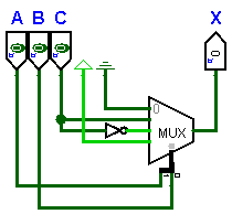
Example 14.4.1. Use a mux to implement a the function, \(F\).

Consider the following truth table.
Table 14.4.2. Truth table for \(F(A, B, C) = AC' + BC\)
\(A\) \(B\) \(C\) \(F\)
\(0\) \(0\) \(0\) \(0\)
\(0\) \(0\) \(1\) \(0\)
\(0\) \(1\) \(0\) \(0\)
\(0\) \(1\) \(1\) \(1\)
\(1\) \(0\) \(0\) \(1\)
\(1\) \(0\) \(1\) \(0\)
\(1\) \(1\) \(0\) \(1\)
\(1\) \(1\) \(1\) \(1\)
  • Convert the truth table for the expression to a function table.
    • Step 1: Use all but the last input as selector lines.
      • In this example, we let \(A\) and \(B\) be used as selector lines.
    • Step 2: Determine the output in terms of the last input.
      • Each row of the function table corresponds to two rows of the truth table. There are only 4 possible binary combinations for a pair of rows that can be expressed in terms of \(C\text{.}\)
Two rows in terms of C
Table 14.4.3. Function table for \(F(A, B, C) = AC' + BC\)
\(A\) \(B\) \(F\)
\(0\) \(0\) \(0\)
\(0\) \(1\) \(C\)
\(1\) \(0\) \(C'\)
\(1\) \(1\) \(1\)
Implement the multiplexor for the function table.
Mux for use a mux for any function example
You have attempted of activities on this page.

Chapter 15 Pre-Lab Exercises

This chapter contains all the pre-lab exercises questions. Your lab instructor will assign questions from this list.

Section 15.1 First Build

Build your first circuit.

Exercises Exercises

1.
(a) Instructions.
Answer all questions in the current section then use the Submit/Check Response button.
  • If your answers are correct then the next section will open.
  • If your answers are incorrect then the next section will not open.
(b) Determine number of rows.
How many rows would be required to make a truth table for the following boolean expressions?
\(O_1\) = \((A + B) \cdot (B + C)\)
\(O_2\) = \((A + C) \cdot (B + C)\)
There are \(n =\) distinct operands, so the truth table needs to have \(2^n =\) rows.
(c) Complete the truth table.
The truth table for
\(O_1\) = \((A + B) \cdot (B + C)\)
\(O_2\) = \((A + C) \cdot (B + C)\)
\(\text{Row}\) \(A\) \(B\) \(C\) \(O_1\) \(O_2\)
\(0\) \(0\) \(0\)
\(1\) \(0\) \(1\)
\(2\) \(1\) \(0\)
\(3\) \(1\) \(1\)
\(4\) \(0\) \(0\)
\(5\) \(1\) \(1\)
\(6\) \(1\) \(1\)
\(7\) \(1\) \(1\)
(d) Choose ICs or chips.
To make a circuit for
\(O_1\) = \((A + B) \cdot (B + C)\)
\(O_2\) = \((A + C) \cdot (B + C)\)
requires:
3 two-input AND gates
2 input AND gate
3 two-input OR gates
2 input OR gate
Indicate the quantity of each chip you need to have access to the required gates:
(e) Choose test values.
Pick three lines from the truth table to use as your test values in lab.
Notes:
Within those test values:
  • every switch (or input) must be set to 0 at least once and to 1 at least once.
  • every LED (or output) must be set to 0 at least once and to 1 at least once.
The subset of rows must be in the correct row number order.
\(\text{Row}\) \(A\) \(B\) \(C\) \(O_1\) \(O_2\)
Hint.
If your test values are incorrect check the criteria carefully.
You have attempted of activities on this page.

Section 15.2 Truth Table to Circuit

Start with a truth table, recognize the correct boolean expression, then plan and build the circuit.

Exercises Exercises

1.
(a) Instructions.
Answer all questions in the current section then use the Submit/Check Response button.
  • If your answers are correct then the next section will open.
  • If your answers are incorrect then the next section will not open.
(b) Determine the boolean expressions.
Consider the following truth table
\(\text{Row}\) \(A\) \(B\) \(C\) \(x\) \(y\)
\(0\) \(0\) \(0\) \(0\) \(0\) \(0\)
\(1\) \(0\) \(0\) \(1\) \(1\) \(0\)
\(2\) \(0\) \(1\) \(0\) \(1\) \(0\)
\(3\) \(0\) \(1\) \(1\) \(0\) \(0\)
\(4\) \(1\) \(0\) \(0\) \(0\) \(0\)
\(5\) \(1\) \(0\) \(1\) \(1\) \(0\)
\(6\) \(1\) \(1\) \(0\) \(1\) \(0\)
\(7\) \(1\) \(1\) \(1\) \(0\) \(1\)
Pick the correct expressions:
(c) Determine the gates.
You can build a circuit for these boolean expressions using \(2\) gates.
Indicate which two gates you need:
2 input AND gate
3 input AND gate
4 input AND gate
2 input OR gate
2 input XOR gate
Hint.
You need to pick one gate for \(x\) and one gate for \(y\text{.}\)
(d) Determine the chips.
Which \(2\) chips correspond to the gates selected in the previous section?
Indicate which chips you need:
(e) Choose test values.
Pick three lines from the truth table to use as your test values in lab.
Notes:
Within those test values:
  • every switch (or input) must be set to 0 at least once and to 1 at least once.
  • every LED (or output) must be set to 0 at least once and to 1 at least once.
The subset of rows must be in the correct row number order.
\(\text{Row}\) \(A\) \(B\) \(C\) \(x\) \(y\)
Hint.
If your test values are incorrect check the criteria carefully.
You have attempted of activities on this page.

Section 15.3 Boolean Expression to Circuit

Start with a boolean expression, make the truth table, then plan and build the circuit.

Exercises Exercises

1.
(a) Instructions.
Answer all questions in the current section then use the Submit/Check Response button.
  • If your answers are correct then the next section will open.
  • If your answers are incorrect then the next section will not open.
(b) Complete the truth table.
\(F_1\) = \(x + y\)
\(F_2\) = \((x \oplus y)'\)
Complete this truth table.
`\text{Row}` `x` `y` `F_1` `F_2`
`0` `0` `0`
`1` `0` `1`
`2` `1` `0`
`3` `1` `1`
(c) Boolean Algebra for \(F_1\).
Put the following statements in order to show how to use algebraic manipulation to change the equation for \(F_1\) to an expression that uses only nands and negation (not).
Reset
(d) Boolean Algebra for \(F_2\).
Put the following statements in order to show how to use algebraic manipulation to change the equation for \(F_2\) to an expression that uses only nands and negation (not).
Reset
(f) Determine the chips.
Which chips correspond to the gates selected in the previous section?
Indicate the quantity of each chip you need:
(g) Choose test values.
Pick three lines from the truth table to use as your test values in lab.
Notes:
Within those test values:
  • every switch (or input) must be set to 0 at least once and to 1 at least once.
  • every LED (or output) must be set to 0 at least once and to 1 at least once.
The subset of rows must be in the correct row number order.
\(\text{Row}\) \(x\) \(y\) \(F_1\) \(F_2\)
Hint.
If your test values are incorrect check the criteria carefully.
You have attempted of activities on this page.

Section 15.4 Build Combinational Circuit

Build a combinational circuit.

Exercises Exercises

1.
(a) Instructions.
Answer all questions in the current section then use the Submit/Check Response button.
  • If your answers are correct then the next section will open.
  • If your answers are incorrect then the next section will not open.
(b) Problem Description.
Design a combinational circuit that takes four inputs (\(E\text{,}\) the enable, and a 3 bit number \(ABC\)), has three outputs (\(XYZ\text{,}\) a three bit number) that meets the following specifications.
  • If \(E = 0\) and \(ABC \ne 111\) then \(XYZ\) should be set to the code after \(ABC\) in this list: \(000, 010, 011, 001, 101, 100, 110, 111\text{.}\)
    • For example, if \(ABC = 001\) then \(XYZ = 101\text{.}\)
    • This is a Gray code sequence. From one value to the next only one bit changes.
  • If \(E = 0\) and \(ABC = 111\text{,}\) then \(XYZ\) may be set to anything (this is called a β€œdon’t care” and should be represented in the truth tables and K-maps with an X).
  • If \(E = 1\) then \(XYZ = ABC\text{.}\)
(c) Truth Table.
Complete this truth table.
`\text{Row}` `E` `A` `B` `C` `X` `Y` `Z`
`0` `0` `0` `0` `0`
`1` `0` `0` `0` `1`
`2` `0` `0` `1` `0`
`3` `0` `0` `1` `1`
`4` `0` `1` `0` `0`
`5` `0` `1` `0` `1`
`6` `0` `1` `1` `0`
`7` `0` `1` `1` `1`
`8` `1` `0` `0` `0`
`9` `1` `0` `0` `1`
`10` `1` `0` `1` `0`
`11` `1` `0` `1` `1`
`12` `1` `1` `0` `0`
`13` `1` `1` `0` `1`
`14` `1` `1` `1` `0`
`15` `1` `1` `1` `1`
Hint.
The problem description is essentially the description of the truth table.
As per the example line 1 of the truth table should read from left to right \(0 0 0 1 1 0 1\text{.}\)
(d) Minterms for `X, Y, Z`.
Complete the expressions below by entering the correct set of values in each space.
  • NOTE: You must enter the values as a set, that is, a comma delimited list inside curly braces.
  • EXAMPLE: \(\{ 0, 1, 2, 3\}\text{.}\)
\(X(E, A, B, C) = \Sigma\) \(, d = \Sigma\)
\(Y(E, A, B, C) = \Sigma\) \(, d = \Sigma\)
\(Z(E, A, B, C) = \Sigma\) \(, d = \Sigma\)
(e) Complete the K-map for `X`.
Complete the K-map for \(X\text{.}\)
X BC B’ B’ B B
EA 00 01 11 10
E’ 00 A’
E’ 01 A
E 11 A
E 01 A’
C’ C C C’
(g) Choose Boolean Expressions for `X`.
Use the Kmap for \(X\) to choose the correct boolean expressions for the essential prime implicants.
(h) Complete the K-map for `Y`.
Complete the K-map for \(Y\text{.}\)
Y BC B’ B’ B B
EA 00 01 11 10
E’ 00 A’
E’ 01 A
E 11 A
E 01 A’
C’ C C C’
(j) Choose Boolean Expressions for `Y`.
Use the Kmap for \(Y\) to choose the correct boolean expressions for the essential prime implicants.
(k) Complete the K-map for `Z`.
Complete the K-map for \(Z\text{.}\)
Z BC B’ B’ B B
EA 00 01 11 10
E’ 00 A’
E’ 01 A
E 11 A
E 01 A’
C’ C C C’
(m) Choose Boolean Expressions for `Z`.
Use the Kmap for \(Z\) to choose the correct boolean expressions for the essential prime implicants.
(n) Determine the gates.
We have determined that
\(X\) = \(A + ((E') \cdot ((B') \cdot C))\)
\(Y\) = \((E \cdot B) + ((E') \cdot (C'))\)
\(Z\) = \(((A') \cdot C) + (((E') \cdot B) + (E \cdot C))\)
Indicate how many of the following gates are required to build a circuit that matches these boolean expressions using distinct chips (that is, at most 1 of each chosen chip).
(o) Determine the chips.
Choose 4 distinct chips to build this circuit.
(p) Choose test values.
Pick three lines from the truth table to use as your test values in lab.
Notes:
Within those test values:
The subset of rows must be in the correct row number order.
\(\text{Row}\) \(E\) \(A\) \(B\) \(C\) \(X\) \(Y\) \(Z\)
Hint.
If your test values are incorrect check the criteria carefully.
You have attempted of activities on this page.

Section 15.5 Adders

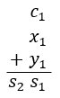
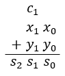
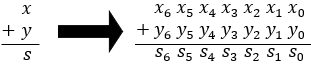
  • The first three questions of this exercise will guide you through creating a two bit adder that corresponds to the equation:
  • You will build this adder by daisy-chaining a 1-bit half adder and a 1-bit full adder.
The format of summing two 2 bit numbers.

Exercises Exercises

1.
(a) Instructions.
Answer all questions in the current section then use the Submit/Check Response button.
  • If your answers are correct then the next section will open.
  • If your answers are incorrect then the next section will not open.
(b) Adding two 1-bit numbers.
What are we trying to do?
We wish to build a circuit that will correctly add the following sums regardless of the order of the values to be added.
Complete the following binary sums:
\(0 + 0 =\)
\(0 + 1 =\)
\(1 + 1 =\)
A circuit that adds two 1-bit binary numbers is called a half-adder.
(c) Complete the truth table.
In digital logic, the outputs of any adder are divided into the sum and the carry-out.
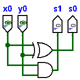
We’re going to label the inputs of our half adder \(a_0\) and \(b_0\text{,}\) the carry-out \(c_1\text{,}\) and the sum \(s_0\text{.}\)
For the sum:
Equation for 1-bit Half Adder
Complete this truth table.
`\text{Row}` `x_0` `y_0` `s_1` `s_0`
`0` `0` `0`
`1` `0` `1`
`2` `1` `0`
`3` `1` `1`
(d) Determine the Gates.
Look up a half adder in your textbook or a reputable website for digital logic, like geeksforgeeks.org.
Indicate which gates are usually used to build a 1-bit half-adder.
2 input AND gate
2 input OR gate
2 input XOR gate
inverter gate
2.
(a) Instructions.
Answer all questions in the current section then use the Submit/Check Response button.
  • If your answers are correct then the next section will open.
  • If your answers are incorrect then the next section will not open.
(b) Adding three 1-bit numbers.
What are we trying to do?
We wish to build a circuit that will correctly add the following sums regardless of the order of the values to be added.
Complete the following binary sums:
\(0 + 0 + 0 =\)
\(0 + 0 + 1 =\)
\(0 + 1 + 1 =\)
\(1 + 1 + 1 =\)
A circuit that adds three 1-bit binary numbers is called a full-adder.
(c) Complete the truth table.
In digital logic, the outputs of any adder are divided into the sum and the carry-out.
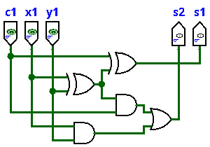
We’re going to label the inputs of our full adder \(c_1\) (the carry-in), \(x_1\) and \(y_1\text{,}\) the carry-out \(s_2\text{,}\) and the sum \(s_1\text{.}\)
For the sum:
Equation for 1-bit Full Adder
Complete this truth table.
`\text{Row}` `c_1` `x_1` `y_1` `s_2` `s_1`
`0` `0` `0` `0`
`1` `0` `0` `1`
`2` `0` `1` `0`
`3` `0` `1` `1`
`4` `1` `0` `0`
`5` `1` `0` `1`
`6` `1` `1` `0`
`7` `1` `1` `1`
(d) Determine the Gates.
Look up a full adder in your textbook or a reputable website for digital logic, like geeksforgeeks.org.
Indicate which gates are usually used to build a 1-bit full-adder.
2 input AND gate
2 input OR gate
2 input XOR gate
inverter gate
3.
(a) Instructions.
Answer all questions in the current section then use the Submit/Check Response button.
  • If your answers are correct then the next section will open.
  • If your answers are incorrect then the next section will not open.
(c) Complete the truth table.
In digital logic, the outputs of any adder are divided into the sum and the carry-out.
We’re going to label the inputs of our full adder \(x_1\text{,}\) \(x_0\text{,}\) \(y_1\text{,}\) and \(y_0\text{,}\) the carry-out \(s_2\text{,}\) and the sum \(s_1\) and \(s_0\text{.}\)
The subscripts indicate the place value of the digit represented by each variable.
So, \(x_0\) has a place value of \(2^0 = 1\text{,}\) \(y_1\) has a place value of \(2^1 = 2\text{,}\) and \(s_2\) has a place value of \(2^2 = 4\text{.}\)
For the sum:
Equation for 2-bit Adder
Complete this truth table.
`\text{Row}` `x_1` `x_0` `y_1` `y_0` `s_2` `s_1` `s_0`
`0` `0` `0` `0` `0`
`1` `0` `0` `0` `1`
`2` `0` `0` `1` `0`
`3` `0` `0` `1` `1`
`4` `0` `1` `0` `0`
`5` `0` `1` `0` `1`
`6` `0` `1` `1` `0`
`7` `0` `1` `1` `1`
`8` `1` `0` `0` `0`
`9` `1` `0` `0` `1`
`10` `1` `0` `1` `0`
`11` `1` `0` `1` `1`
`12` `1` `1` `0` `0`
`13` `1` `1` `0` `1`
`14` `1` `1` `1` `0`
`15` `1` `1` `1` `1`
(d) Determine the Gates.
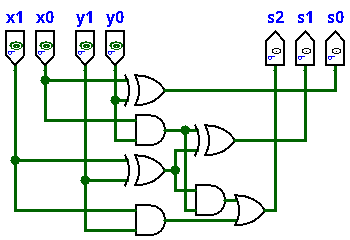
To daisy-chain the half and full adders, we connect the carry-out (the output \(c_1\)) of the half adder to the carry-in (the input \(c_1\)) of the full adder.
Indicate which gates will be required to build this circuit.
2 input AND gate
2 input OR gate
2 input XOR gate
inverter gate
(e) Determine the chips.
This is a logic circuit for a 2-bit adder.
2-bit Adder Logic Circuit
How many of the chips below do we need to build the wiring diagram that corresponds to this logic circuit?
(f) Choose test values.
Pick three lines from the truth table to use as your test values in lab.
Include the base 10 equivalent of the binary values.
Notes:
Within those test values:
  • every switch (or input) must be set to 0 at least once and to 1 at least once.
  • every LED (or output) must be set to 0 at least once and to 1 at least once.
  • do not test the rows with don’t cares.
The subset of rows must be in the correct row number order.
\(\text{Row}\) \(x_1\) \(x_0\) \(y_1\) \(y_0\) \(s_2\) \(s_1\) \(s_0\) \(x\) (base 10) \(y\) (base 10) \(s\) (base 10)
Hint.
If your test values are incorrect check the criteria carefully.
4.
(a) Instructions.
Answer all questions in the current section then use the Submit/Check Response button.
  • If your answers are correct then the next section will open.
  • If your answers are incorrect then the next section will not open.
(b) Adding two 7-bit binary numbers.
What are we trying to do?
We wish to build a circuit that will correctly add two 7-bit two’s complement numbers.
Equation for 7-bit Adder
This is too large a problem for us to want to create a truth table.
If we made a truth table for this circuit, it would have \(2^{n}\) rows where \(n=\) .
We do not have the resources to daisy chain another five 1-bit full-adders to the circuit for Problem 3 so we need to use two 74LS283 4-Bit Full Adder chips.
Your kit only has one 74LS283 4-Bit Full Adder chip so you will work in pairs to build this circuit in lab.
(c) Investigation of the 74LS283 chip.
Consult the lab manual to determine how the 74LS283 chip is used.
Indicate how you must contect the 74LS283 chips to implement this adder.
Notes:
  • You must daisy chain the two chips appropriately.
  • Use Chip 1 to sum \(x_6, x_5, x_4\) with \(y_6, y_5, y_4\) respectively.
  • Use Chip 2 to sum \(x_3, x_2, x_1, x_0\) with \(y_3, y_2, y_1, y_0\) respectively.
  • All input pins on the chip must be connected to something.
  • Unused output pins do not need to be connected to anything, choose \(\phi\) to indicate the pins is not connected to anything.
  • Use ground for constant 0 and power for constant 1.
Chip 1:
grd
16 15 14 13 12 11 10 9
\(B3\) \(A3\) \(\Sigma3\) \(A4\) \(B4\) \(\Sigma4\) \(C4_1\)
\(\cdot\) \(-\) \(-\) \(-\) \(-\) \(-\) \(-\) \(\cdot\)
| 74 LS 283 Chp 1 |
\(\cdot\) \(-\) \(-\) \(-\) \(-\) \(-\) \(-\) \(\cdot\)
\(\Sigma2\) \(B2\) \(A2\) \(\Sigma1\) \(A1\) \(B1\) \(C0_1\)
1 2 3 4 5 6 7 8
Chip 2:
grd
16 15 14 13 12 11 10 9
\(B3\) \(A3\) \(\Sigma3\) \(A4\) \(B4\) \(\Sigma4\) \(C4_2\)
\(\cdot\) \(-\) \(-\) \(-\) \(-\) \(-\) \(-\) \(\cdot\)
| 74 LS 283 Chp 2 |
\(\cdot\) \(-\) \(-\) \(-\) \(-\) \(-\) \(-\) \(\cdot\)
\(\Sigma2\) \(B2\) \(A2\) \(\Sigma1\) \(A1\) \(B1\) \(C0_2\)
1 2 3 4 5 6 7 8
(d) Choose test values.
Here are four sets of test values to show that your adder works correctly.
These test values are chosen so that:
  • every switch (or input) must be set to 0 at least once and to 1 at least once.
  • every LED (or output) must be set to 0 at least once and to 1 at least once.
  • at least one of the tests sets \(C4_2\) to one and at least one of the tests should set \(C4_2\) to zero.
Note:
  • \(x_6x_5x_4x_3x_2x_1x_0\text{,}\) \(y_6y_5y_4y_3y_2y_1y_0\text{,}\) and \(s_6s_5s_4s_3s_2s_1s_0\) are 7 bit two’s complement values
  • \(x\text{,}\) \(y\text{,}\) and \(s\) are signed decimal integers that are equivalent to \(x_6x_5x_4x_3x_2x_1x_0\text{,}\) \(y_6y_5y_4y_3y_2y_1y_0\text{,}\) and \(s_6s_5s_4s_3s_2s_1s_0\) respectively.
Indicate the decimal equivalent for each 7 bit two’s complement value.
\(x_6x_5x_4x_3x_2x_1x_0\) \(y_6y_5y_4y_3y_2y_1y_0\) \(s_6s_5s_4s_3s_2s_1s_0\) \(x\) \(y\) \(s\)
0 0 0 0 0 0 0 1 1 1 1 1 1 1 1 1 1 1 1 1 1
1 1 1 1 1 1 1 0 0 0 0 0 0 0 1 1 1 1 1 1 1
0 0 0 1 1 1 1 0 0 0 0 0 0 1 0 0 1 0 0 0 0
0 1 1 1 1 1 1 1 0 0 0 0 0 1 0 0 0 0 0 0 0
Hint.
There are two’s complement to decimal calculators online.
You have attempted of activities on this page.

Section 15.6 Decoders

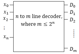
A decoder is a combinational circuit that converts an \(n\) bit code to one of \(m \le 2^n\) possible output lines.
Generic Decoder

Exercises Exercises

1.
(a) Instructions.
Answer all questions in the current section then use the Submit/Check Response button.
  • If your answers are correct then the next section will open.
  • If your answers are incorrect then the next section will not open.
(b) Complete the truth table.
Use the same method as seen in the β€œExample: 2-to-4 Decoder” section (above) to make a 3-to-8 Decoder that accepts a \(3\)-digit binary number (\(d_2d_1d_0\)) as input and indicates the equivalent decimal number by lighting the correct LED (\(L_0\) to \(L_7\)).
Complete the truth table.
`\text{Row}` `d_2` `d_1` `d_0` `L_0` `L_1` `L_2` `L_3` `L_4` `L_5` `L_6` `L_7`
`0` `0` `0` `0`
`1` `0` `0` `1`
`2` `0` `1` `0`
`3` `0` `1` `1`
`4` `1` `0` `0`
`5` `1` `0` `1`
`6` `1` `1` `0`
`7` `1` `1` `1`
Hint.
The LED labelled \(L_x\) should be on/high/\(1\) when \(d_2 \times 2^2 + d_1 \times 2^1 + d_0 \times 2^0 = x\) and off/low/\(0\) in all the other rows.
(c) Boolean Expressions for \(L_0\) to \(L_7\).
Put the following expressions in order so that the first one is the expression for \(L_0\text{,}\) the second for \(L_1\text{,}\) and so on until the expression for \(L_7\text{.}\)
Reset
(d) Determine the gates.
Indicate how many of the following gates are required to build the 3-to-8 decoder.
3-input AND gate
inverter gate
(e) Limited resources.
Unfortunately, the kit doesn’t have enough of the chips with \(3\)-input AND gates to make this circuit with eight 3-input AND gates.
However, from the Boolean Algebra we know the following are all equivalent.
\(\displaystyle{x \cdot y \cdot z }\)\(\displaystyle{= x \cdot (y \cdot z) = (x \cdot y) \cdot z = (x \cdot z) \cdot y = y \cdot (x \cdot z)}\) ...
\(\displaystyle{= x \cdot x \cdot y \cdot z = x \cdot y \cdot y \cdot z}\) ...
\(\displaystyle{= 1 \cdot x \cdot y \cdot z = x \cdot y \cdot z \cdot 1}\) ...
Hence, we can use the following gate combinations when we are β€œANDing” three inputs.
What is the MAXIMUM number of each gate combination that can be built usingthe chips in the kit?
3-input AND gate
Two 2-input AND gates
4-input AND gate
(f) Determine the chips.
How many of the following chips do you need to use to make the 3-to-8 decoder with inverters and AND gates?
(g) Consider test values.
Within our test values we want:
  • every switch (or input) must be set to 0 at least once and to 1 at least once.
  • every LED (or output) must be set to 0 at least once and to 1 at least once.
How many test values must you show to meet this criteria?
2.
(a) Instructions.
Answer all questions in the current section then use the Submit/Check Response button.
  • If your answers are correct then the next section will open.
  • If your answers are incorrect then the next section will not open.
(b) Investigation of the 74LS139 chip.
First consider how to build a \(2 \rightarrow 4\) decoder using the 74LS139 Dual\(2 \rightarrow 4\) Decoder chip.
Read about the chip in the lab kit manual.
If you wanted to use side 1 (the bottom half in the picture) to implement a \(2 \rightarrow 4\) decoder for the inputs \(d_1, d_0\) and outputs \(L_0, L_1, L_2, L_3\text{,}\) how would you connect the pins \(1\) to \(7\text{?}\)
grd
\(\circ\) \(\circ\) \(\circ\) \(\circ\) \(\circ\) \(\circ\) \(\circ\)
16 15 14 13 12 11 10 9
\(\overline{E}_2\) \(B_2\) \(A_2\) \(Y_0\) \(Y_1\) \(Y_3\) \(Y_4\)
\(\cdot\) \(-\) \(-\) \(-\) \(-\) \(-\) \(-\) \(\cdot\)
| 74 LS 139 N |
\(\cdot\) \(-\) \(-\) \(-\) \(-\) \(-\) \(-\) \(\cdot\)
\(\overline{E}_1\) \(B_1\) \(A_1\) \(X_0\) \(X_1\) \(X_2\) \(X_3\)
1 2 3 4 5 6 7 8
(c) Complete the truth table for using the \(2 \rightarrow 4\) Decoder Chip.
Using what you learned in the Lab Kit Manual.
Complete the truth table to reflect what the chip would do.
`\text{Row}` `d_1` `d_0` `L_0` `L_1` `L_2` `L_3`
`0` `0` `0`
`1` `0` `1`
`2` `1` `0`
`3` `1` `1`
(d) Complete the truth table for the \(3 \rightarrow 8\) decoder.
In the lab kit manual it describes how to use the 74LS139 chip to make a \(3 \rightarrow 8\) decoder.
Based on the truth table from the previous section, what do you expect the truth table for the \(3 \rightarrow 8\) decoder made with the 74LS139 chip will look like?
`\text{Row}` `d_2` `d_1` `d_0` `L_0` `L_1` `L_2` `L_3` `L_4` `L_5` `L_6` `L_7`
`0` `0` `0` `0`
`1` `0` `0` `1`
`2` `0` `1` `0`
`3` `0` `1` `1`
`4` `1` `0` `0`
`5` `1` `0` `1`
`6` `1` `1` `0`
`7` `1` `1` `1`
(e) Further investigation of the 74LS139 chip.
Following the instructions in the lab manual, fill in the missing connections, for all the pins, you’ll need to use the 74LS139 Dual \(2 \rightarrow 4\) Decoder chip to build a 3->8 decoder.
grd
16 15 14 13 12 11 10 9
\(\overline{E}_2\) \(B_2\) \(A_2\) \(Y_0\) \(Y_1\) \(Y_3\) \(Y_4\)
\(\cdot\) \(-\) \(-\) \(-\) \(-\) \(-\) \(-\) \(\cdot\)
| 74 LS 139 N |
\(\cdot\) \(-\) \(-\) \(-\) \(-\) \(-\) \(-\) \(\cdot\)
\(\overline{E}_1\) \(B_1\) \(A_1\) \(X_0\) \(X_1\) \(X_2\) \(X_3\)
1 2 3 4 5 6 7 8
\(d_0\) \(d_1\) \(L_0\) \(L_1\) \(L_2\) \(L_3\)
(f) Determine the chips.
How many of the following chips do you need to use to make a \(3 \rightarrow 8\) decoder with inverters and two \(2 \rightarrow 4\) decoders?
(g) Consider test values.
Within our test values we want:
  • every switch (or input) must be set to 0 at least once and to 1 at least once.
  • every LED (or output) must be set to 0 at least once and to 1 at least once.
How many test values must you show to meet this criteria?
You have attempted of activities on this page.

Section 15.7 Multiplexors

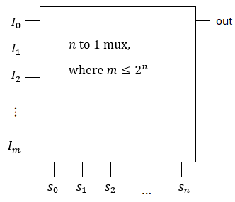
A mux has two types of input and one output.
Generic Mux

Exercises Exercises

1.
(a) Instructions.
Answer all questions in the current section then use the Submit/Check Response button.
  • If your answers are correct then the next section will open.
  • If your answers are incorrect then the next section will not open.
(b) Truth table for a two-to-one mux.
For a two-to-one multiplexor when:
Complete this truth table.
`\text{Row}` `s` `I_0` `I_1` `out`
`0` `0` `0` `0`
`1` `0` `0` `1`
`2` `0` `1` `0`
`3` `0` `1` `1`
`4` `1` `0` `0`
`5` `1` `0` `1`
`6` `1` `1` `0`
`7` `1` `1` `1`
(c) K-map for a two-to-one mux.
Complete the K-map for \(O\text{.}\)
\(O\) \(I_0I_1\) \(I_0'\) \(I_0'\) \(I_0\) \(I_0\)
\(s\) \(00\) \(01\) \(11\) \(10\)
\(s'\) \(0\)
\(s\) \(1\)
\(I_1'\) \(I_1\) \(I_1\) \(I_1'\)
(d) Prime implicants for \(O\).
Use the K-map to determine the essential prime implicants for \(O\text{.}\)
(e) Function table for two-to-one mux.
A truth table is a very long winded way of describing a mux.
Instead we can use a function table, in the function table we indicate how to determine the output (a function) for each possible value of the selector line(s). In this case, the function is simply the variable in control.
In the \(O\) column indicate which input line has control of the output.
\(s\) \(O\)
\(0\)
\(1\)
(f) Investigate the 74LS157 chip.
From the boolean expressions we obtain the following logic circuit:
2-to-1 Mux in simple gates
But we don’t need to build this typically, a mux is depicted in a logic circuit like this:
2-to-1 Mux gate
The 74LS157 chip has four 2-to-1 Multiplexors available.
Read about the 74LS157 chip in the lab manual.
If we wanted to build the Mux represented by the image above using Mutliplexor 3 (a two-to-one mux) of the 74LS157 chip what would you connect to the following pins?
pwr
\(\:\phi\:\) \(\:\phi\:\) \(\:\phi\:\)
16 15 14 13 12 11 10 9
\(\overline{E}\) \(4A\) \(4B\) \(4O\) \(3A\) \(3B\) \(3O\)
\(\:\cdot\:\) \(\:-\:\) \(\:-\:\) \(\:-\:\) \(\:-\:\) \(\:-\:\) \(\:-\:\) \(\:\cdot\:\)
\(\:\)|\(\:\) \(\:\:\:\) \(\:\:\:\) \(\:\)1\(\:\) \(\:\)5\(\:\) \(\:\)7\(\:\) \(\:\:\:\) \(\:\)|\(\:\)
\(\:\cdot\:\) \(\:-\:\) \(\:-\:\) \(\:-\:\) \(\:-\:\) \(\:-\:\) \(\:-\:\) \(\:\cdot\:\)
\(S\) \(1A\) \(1B\) \(1O\) \(2A\) \(2B\) \(2O\)
1 2 3 4 5 6 7 8
\(\:\phi\:\) \(\:\phi\:\) \(\:\phi\:\) \(\:\phi\:\) \(\:\phi\:\) \(\:\phi\:\)
2.
(a) Instructions.
Answer all questions in the current section then use the Submit/Check Response button.
  • If your answers are correct then the next section will open.
  • If your answers are incorrect then the next section will not open.
(b) Truth table for four-to-one mux.
Suppose we have a four-to-one mux with ...
Demonstrate your understanding of what a multiplexor accomplishes by completing this truth table:
\(s_1\) \(s_0\) \(I_0\) \(I_1\) \(I_2\) \(I_3\) \(O\)
\(0\) \(0\) \(0\) X X X
\(0\) \(0\) \(1\) X X X
\(0\) \(1\) X \(0\) X X
\(0\) \(1\) X \(1\) X X
\(1\) \(0\) X X \(0\) X
\(1\) \(0\) X X \(1\) X
\(1\) \(1\) X X X \(0\)
\(1\) \(1\) X X X \(1\)
(c) Function table for four-to-one mux.
Complete the function table for this mux.
In the \(O\) column indicate which input line has control of the output.
\(s_1\) \(s_0\) \(O\)
\(0\) \(0\)
\(0\) \(1\)
\(1\) \(0\)
\(1\) \(1\)
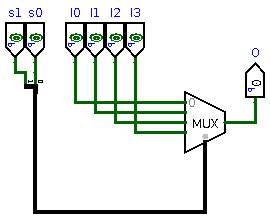
(d) Make a 4-to-1 mux with 2-to-1 muxes.
If we use a 4-to-1 multiplexor gate to make a logic circuit for this exercise it would look like this:
t-to-1 Mux gate
However, we don’t have a chip with a 4-to-1 mux.
How can we use 2-to-1 multiplexors to make a 4-to-1 multiplexor.
Consider the selector lines one at a time.
\(s_1\)
\(0\)
\(1\)
  • For the top half, \(s_1 = 0\) and \(s_0\) chooses between \(I_0\) and \(I_1\text{.}\)
  • For the bottom half, \(s_1 = 1\) and \(s_0\) chooses between \(I_2\) and \(I_3\text{.}\)
  • Lastly, the selector line \(s_1\) chooses between the top half of the table and the bottom half of the table.
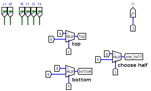
Hence, we get the following tables for each multiplexor:
We create a 2-to-1 mux for each of these three tables.
Indicate how this logic circuit should be wired by matching the inputs and outputs of each mux to the switches, led, and gates.
4-to-1 Matching Mux
a f
b g
c h
d i
e j
(e) Investigate the 74LS157 chip.
We must use two 74LS157 chips for this circuit because all the muxes on one chip are connected to the same selector line.
Since we have two selector lines we must have two chips.
Choose the correct connections for the two 74LS157 chips:
Assume:
  • For the multiplexors labelled β€œtop,” β€œbottom,” and β€œchoose half” in the previous section, use Multiplexor 4 and 3 on the first chip and Multiplexor 4 on the second chip, respectively.
First 74LS157 Chip Use Mux 4 for β€œtop” and Mux 3 for β€œbottom.”
pwr
16 15 14 13 12 11 10 9
\(\overline{E}\) \(4A_1\) \(4B_1\) \(4O_1\) \(3A_1\) \(3B_1\) \(3O_1\)
\(\cdot\) \(-\) \(-\) \(-\) \(-\) \(-\) \(-\) \(\cdot\)
| 1 5 7 ~ Chp 1 |
\(\cdot\) \(-\) \(-\) \(-\) \(-\) \(-\) \(-\) \(\cdot\)
\(S\) \(1A_1\) \(1B_1\) \(1O_1\) \(2A_1\) \(2B_1\) \(2O_1\)
1 2 3 4 5 6 7 8
\(\phi\) \(\phi\) \(\phi\) \(\phi\) \(\phi\) \(\phi\)
Second 74LS157 Chip Use Mux 4 for β€œchoose half.”
pwr
\(\phi\) \(\phi\) \(\phi\)
16 15 14 13 12 11 10 9
\(\overline{E}\) \(4A_2\) \(4B_2\) \(4O_2\) \(3A_2\) \(3B_2\) \(3O_2\)
\(\cdot\) \(-\) \(-\) \(-\) \(-\) \(-\) \(-\) \(\cdot\)
| 1 5 7 ~ Chp 2 |
\(\cdot\) \(-\) \(-\) \(-\) \(-\) \(-\) \(-\) \(\cdot\)
\(S\) \(1A_2\) \(1B_2\) \(1O_2\) \(2A_2\) \(2B_2\) \(2O_2\)
1 2 3 4 5 6 7 8
\(\phi\) \(\phi\) \(\phi\) \(\phi\) \(\phi\) \(\phi\)
(f) Choose test values.
Pick four sets of test values to use in lab.
Within those test values:
Multiplexor testing: make sure there is at least one test for each possible value of the selector lines.
The subset of rows must be in the correct row number order.
\(s_1\) \(s_0\) \(I_0\) \(I_1\) \(I_2\) \(I_3\) \(O\)
Hint.
If your test values are incorrect check the criteria carefully.
3.
(a) Instructions.
Answer all questions in the current section then use the Submit/Check Response button.
  • If your answers are correct then the next section will open.
  • If your answers are incorrect then the next section will not open.
(b) Make the truth table.
A communications company wants to encode all its data before transmitting it. Design a circuit to assist them with this encoding. Every unsigned 3-bit binary number, \(n_2n_1n_0\) (base 2) = \(N\)(base 10), will be encoded by adding a fourth binary digit \(X\text{.}\) The encoding works as follows:
  • If \(N \% 4 = 3\) then the 4 digit binary number transmitted, \(n_2n_1n_0X\) must have odd parity.
  • If \(N \% 4 \ne 3\) then the 4 digit binary number transmitted, \(n_2n_1n_0X\) must have even parity.
  • So, each number transmitted will have 4 bits, the 3 bits of the unsigned binary number and \(X\text{.}\)
Complete the truth table (with extra leading columns) showing the number \(N\) (base 10), \(N\%4\text{,}\) whether the parity should be odd or even, inputs \(n_2\text{,}\) \(n_1\text{,}\) \(n_0\text{,}\) and output \(X\)
  • Notes:
    • A binary number has even parity if it contains an even number of ones and odd parity if it contains an odd number of ones.
    • \(N \% 4\) is the remainder when you divide by four. The remainder must be between \(0\) and \(3\text{,}\) inclusive.
\(N_{10}\) \(N \% 4\) parity \(n_2\) \(n_1\) \(n_0\) \(X\)
0
1
2
3
4
5
6
7
(c) Complete the K-map.
\(X\) \(n_1n_0\) \(n_1'\) \(n_1'\) \(n_1\) \(n_1\)
\(n_2\) \(00\) \(01\) \(11\) \(10\)
\(n_2'\) \(0\)
\(n_2\) \(1\)
\(n_0'\) \(n_0\) \(n_0\) \(n_0'\)
How many groups of which size can be circled to determine the prime implicants?
(d) Prime implicants for \(X\).
Use the K-map to determine the essential prime implicants for \(X\text{.}\)
(e) Make the function table.
We’re going to implement this circuit using multiplexors.
Complete the function table for \(X\text{.}\)
\(n_2\) \(n_1\) \(X\)
(f) Determine the chips.
How many of the following chips do you need to use to make this circuit?
(g) Choose test values.
Pick four sets of test values to use in lab.
Within those test values:
Multiplexor testing: make sure there is at least one test for each possible value of the selector lines.
The subset of rows must be in ascending order.
\(n_2\) \(n_1\) \(n_0\) \(n_2\) \(n_1\) \(n_0\) \(X\)
Hint.
If your test values are incorrect check the criteria carefully.
  • Do the row numbers match the values for the input columns in the full truth table?
  • Are the rows in ascending order by input values?
  • Does each column contain at least one 0?
  • Does each column contain at least one 1?
  • Is there an X, which represents a don’t care, in any row?
  • Is there a test for each possible value for the selector lines \(n_2\) and \(n_1\text{?}\)
  • Do the input and output values for \(n_2\text{,}\) \(n_1\text{,}\) and \(n_0\) match in every row?
  • Still not correct... click on the red box next to the table and check for an error message.
You have attempted of activities on this page.

Section 15.8 Latches and Flip Flops

A latch stores data, protects data, has a method to access data, and has a method to update data. A latch with input control can lock the data to prevent it from being overwritten.

Exercises Exercises

1.
(a) Instructions.
Answer all questions in the current section then use the Submit/Check Response button.
  • If your answers are correct then the next section will open.
  • If your answers are incorrect then the next section will not open.
(b) State table for an SR Latch with input control.
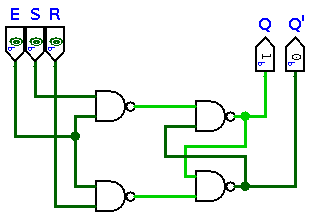
This is an SR-Latch with input control.
SR Latch
It can be used to store 1 bit of data.
Complete the following state table, \(Q+\) is the next state seen if the values of \(E, S, R,\) and \(Q\) are set as given.
\(E\) \(S\) \(R\) \(Q\) \(Q+\)
\(0\) \(0\) \(0\) \(0\)
\(0\) \(0\) \(0\) \(1\)
\(0\) \(0\) \(1\) \(0\)
\(0\) \(0\) \(1\) \(1\)
\(0\) \(1\) \(0\) \(0\)
\(0\) \(1\) \(0\) \(1\)
\(0\) \(1\) \(1\) \(0\)
\(0\) \(1\) \(1\) \(1\)
\(1\) \(0\) \(0\) \(0\)
\(1\) \(0\) \(0\) \(1\)
\(1\) \(0\) \(1\) \(0\)
\(1\) \(0\) \(1\) \(1\)
\(1\) \(1\) \(0\) \(0\)
\(1\) \(1\) \(0\) \(1\)
\(1\) \(1\) \(1\) \(0\)
\(1\) \(1\) \(1\) \(1\)
(c) Condensed state table for an SR Latch with input control.
Adjacent lines of the state table that can be described using don’t cares, have the same reason for the next state, and the value of \(Q+\) can be described as a constant or a function can be condensed to one line of the table.
\(E\) \(S\) \(R\) \(Q\) \(Q+\)
\(0\) \(\text{X}\) \(\text{X}\) \(\text{X}\)
\(1\) \(0\) \(0\) \(\text{X}\)
\(1\) \(0\) \(1\) \(\text{X}\)
\(1\) \(1\) \(0\) \(\text{X}\)
\(1\) \(1\) \(1\) \(\text{X}\)
(d) Differences between SR-Latch and D-Latch.
A D-Latch is similar to an SR-Latch but it eliminates the possiblility of an indeterminte state.
SR Latch
To change this SR Latch to a D Latch with input control what must be done?
(e) State table for an D Latch with input control.
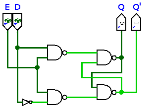
This is a D Latch with input control.
D Latch
\(D\) is the data switch.
To determine the state table for the D Latch.
How many input columns should be in the D Latch’s state table?
How many rows should be in the D Latch’s uncondensed state table?
(f) Complete the state table.
Complete the following state table, \(Q+\) is the next state seen if the values of \(E, D,\) and \(Q\) are set as given.
\(E\) \(D\) \(Q\) \(Q+\)
\(0\) \(0\) \(0\)
\(0\) \(0\) \(1\)
\(0\) \(1\) \(0\)
\(0\) \(1\) \(1\)
\(1\) \(0\) \(0\)
\(1\) \(0\) \(1\)
\(1\) \(1\) \(0\)
\(1\) \(1\) \(1\)
If we condense adjacent lines of this table in the same manner we did for the SR-Latch, how many rows would the condensed state table have?
(g) Condensed state table for an D Latch with input control.
Adjacent lines of the state table that can be described using don’t cares, have the same reason for the next state, and the value of \(Q+\) can be described as a constant or a function can be condensed to one line of the table.
\(E\) \(D\) \(Q\) \(Q+\)
\(0\) \(\text{X}\) \(\text{X}\)
\(1\) \(0\) \(\text{X}\)
\(1\) \(1\) \(\text{X}\)
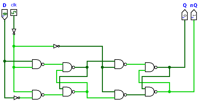
(h) Negative Edge to Positive Edge.
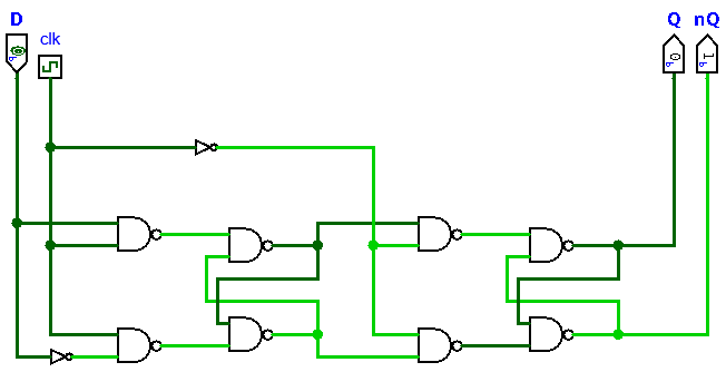
This is a negative edge leader-follower D flip-flop.
  • The flip-flop is constructed using two D Latches.
  • The first latch updates when the clock is high.
  • Hence ...
    • If the clock is high then the first latch updates when D is changed.
    • If the clock is low then the first latch updates on the clock’s positive edge, that is, when the clock becomes high.
  • The second latch updates on the first negative edge after the first latch is updated.
D Flip-flop
You can change this to a positive edge leader-follower D flip-flop by adding one gate.
Which of the following gates should be added?
ID Gate ID Gate
NOT
1 in NOT gate
OR
2 in OR gate
XOR
2 in XOR gate
NOR
2 in NOR gate
AND
2 in AND gate
NAND
D Flip-flop
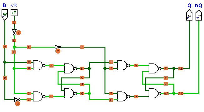
(i) Optimize a little.
This positive edge leader-follower D flip-flop can be built with one less inverter than is shown.
D Flip-flop
We can remove two of the inverters and add one in a new location.
Can you see where?
Which two inverters shown in the image below should be removed?
D Flip-flop
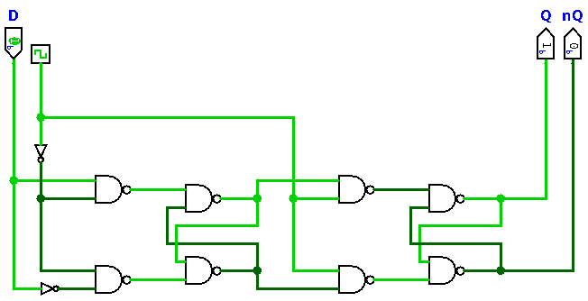
(j) Positive Edge leader-follower D flip-flop description.
D Flip-flop
Complete the description of a positive edge leader-follower D flip-flop.
Hint.
Refer to the description of a negative edge leader-follower D flip-flop above.
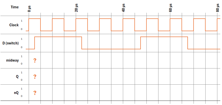
(k) Complete the timing diagram.
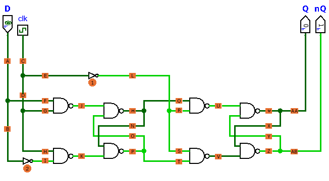
This is a Posative Edge Leader Follower D flip-flop.
D Flip-flop
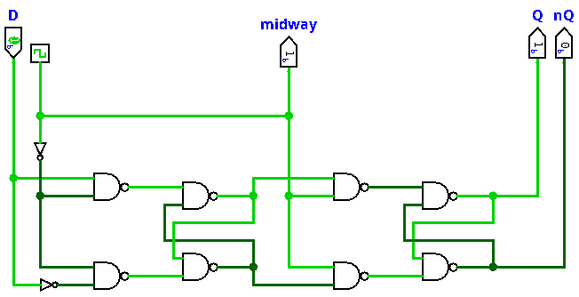
Consider the following partial timing diagram:
D Flip-flop
Determine when each tracked signal changes.
The time that the \(D\) switch changes is listed below, when does the value of midway, \(Q\text{,}\) and \(nQ\) (which is \(Q'\)) change?
\(D\) switch midway \(Q\) \(nQ\)
\(2 \mu s\) at \(\mu s\text{,}\) midway = at \(\mu s, Q =\) at \(\mu s, nQ =\)
\(22 \mu s\) at \(\mu s\text{,}\) midway = at \(\mu s, Q =\) at \(\mu s, nQ =\)
\(47 \mu s\) at \(\mu s\text{,}\) midway = at \(\mu s, Q =\) at \(\mu s, nQ =\)
\(67 \mu s\) at \(\mu s\text{,}\) midway = at \(\mu s, Q =\) at \(\mu s, nQ =\)
You have attempted of activities on this page.

Section 15.9 Use a D MemoryChip

The D memory chip uses four D flip flops to store 4 bits of data.

Exercises Exercises

1.
(a) Instructions.
Answer all questions in the current section then use the Submit/Check Response button.
  • If your answers are correct then the next section will open.
  • If your answers are incorrect then the next section will not open.
(b) D Memory chip and the clock.
Read about the 74LS175 β€œD” Memory Chip and the clock in the lab manual then complete the following sentences.
(c) Complete the state table.
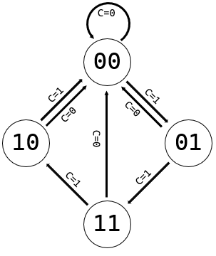
This is the state diagram for the 2-bit greycode counter you will build.
2 bit Grey Code State Diagram
  • The circles contain all the possible states for our circuit.
    • For our circuit this is all the possible combinations of values that we want to store in memory.
  • The arrows show the next state, if the next state depends on an input value then the variable and the value are displayed next to the arrow.
So, if the current value is \(AB = 01\) then when \(C = 1\) the next value \(A^+B^+ = 11\text{.}\)
Use the information in the state diagram to complete the state table, for the moment only pay attention to the \(C = 1\) arrows.
`\text{Row}` `A` `B` `A^+` `B^+`
`0` `0` `0`
`1` `0` `1`
`2` `1` `0`
`3` `1` `1`
(d) Boolean expressions for \(A^+, B^+\).
The boolean expressions for \(A^+\) and \(B^+\) are easily determined by observation.
Compare the output columns to the input columns.
\(A^+ =\)
\(B^+ =\)
(e) Investigate the 74LS175 chip.
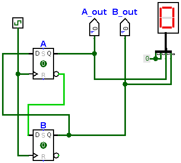
This is the logic circuit for the 2-bit grey-code counter we looked at earlier in this question.
2 bit Grey Code Counter
To build this we need to use the 74LS175 Quad β€œD” Memory chip.
On the chip there is a \(\overline{\text{clr}}\) which will clear all the memory bits when it is low. This is where the \(C\) you saw in the state diagram comes into our build. Make an input pin (switch) for \(C\) and use it to clear the memory when appropriate.
Indicate what each pin of the 74LS175 Quad β€œD” Memory chip depicted below should be connected to make the wiring diagram for this circuit. Use D flip-flop 4 for \(A\) and D flip-flop 3 for \(B\text{.}\) Use \(\phi\) to indicate a pin doesn’t need to be connected to anything.
Note: once everything is correctly set up to store and update the two bits of memory, connect the outputs so that you can see what is happening in memory.
pwr
16 15 14 13 12 11 10 9
\(4Q\) \(4\overline{Q}\) \(4D\) \(3D\) \(3\overline{Q}\) \(3Q\) clk
\(\,\)
. _ _ _ _ _ _ .
| 1 7 5 |
\(\dot{\,}\) \(\overline{\,}\) \(\overline{\,}\) \(\overline{\,}\) \(\overline{\,}\) \(\overline{\,}\) \(\overline{\,}\) \(\dot{\,}\)
\(\,\)
\(\overline{\text{clr}}\) \(1Q\) \(1\overline{Q}\) \(1D\) \(2D\) \(2\overline{Q}\) \(2Q\)
1 2 3 4 5 6 7 8
\(\phi\) \(\phi\) \(\phi\) \(\phi\) \(\phi\) \(\phi\)
(f) Determine the chips.
How many of the following chips do you need to use to make this circuit?
74LS00 Quad 2-input NAND Gate 74LS02 Quad 2-input NOR Gate
74LS04 Hex inverter 74LS08 Quad 2-input AND Gate
74LS10 Triple 3-input NAND Gate 74LS11 Triple 3-input AND Gate
74LS20 Dual 4-input NAND Gate 74LS21 Dual 4-input AND Gate
74LS27 Triple 3-input NOR Gate 74LS32 Quad 2-input OR Gate
74LS86 Quad 2-input Exclusive-OR Gate 74LS139 Dual 2->4 Decoder
74LS157 Quad 1-of-2 Multiplexor 74LS175 Quad ’D’ Memory
74LS283 4-Bit Full Adder 74LS670 4x4 Register File
You have attempted of activities on this page.

Section 15.10 Build a Counter

This counter will use the clock to run.

Exercises Exercises

1.
(a) Instructions.
Answer all questions in the current section then use the Submit/Check Response button.
  • If your answers are correct then the next section will open.
  • If your answers are incorrect then the next section will not open.
(b) Handy Notes: Basic Rules of Boolean Algebra.
Basic Theorems and Properties of Boolean Algebra\(^1\)
----------------------------- ----------------------------------- ------------------------------------
Postulate 2 \(x+0=x\) \(x \cdot 1=x\)
Postulate 5 \(x+x’=1\) \(x \cdot x’=0\)
Theorem 1 \(x+x=x\) \(x \cdot x=x\)
Theorem 2 \(x+1=1\) \(x \cdot 0=0\)
Theorem 3 involution \((x’)’=x\)
Postulate 3, commutative \(x+y=y+x\) \(x \cdot y=y \cdot x\)
Theorem 4, associative \(x+(y+z)=(x+y)+z\) \(x \cdot (y \cdot z)=(x \cdot y) \cdot z\)
Postulate 4, distributive \(x \cdot (y+z)=x \cdot y+x \cdot z\) \(x+(y \cdot z)=(x+y) \cdot (x+z)\)
Theorem 5, DeMorgan \((x+y)’=x’ \cdot y’\) \((x \cdot y)’=x’+y’\)
Theorem 6, absorption \(x+xy=x\) \(x(x+y)=x\)
----------------------------- ----------------------------------- -----------------------------------
Additional Rules and Theorems
----------------------------- ----------------------------------- ------------------------------------
Identities \(x+0=x\) \(x \cdot 1=x\)
----------------------------- ----------------------------------- ------------------------------------
Definitions
----------------------------- ----------------------------------------------------------------------------
NAND \(x \text{ nand } y=(x \cdot y)’\)
NOR \(x \text{ nor } y=(x+y)’\)
XOR (exclusive or) \(xβŠ•y=(x \cdot y’ )+(x’ \cdot y) =(x+y) \cdot (x’+y’)\)
----------------------------- ----------------------------------------------------------------------------
  1. Mano, M. Morris and Ciletti. Digital Design. 5th. New Jersey: Pearson Education, 2013. Book.
(c) Complete the state table.
Make a counter that counts from \(0000\) \((0)\) to \(1111\) \((F)\text{,}\) repeatedly when \(R = 1\) and display \(0000\) \((0)\) when \(R = 0\text{.}\)
This is a state diagram showing all the states for our counter circuit and how they relate to each other.
4 bit Counter state diagram
You will use D-memory and the clock to build this circuit.
First we need to determine the boolean expressions for determining the next value in the sequence.
Let \(N = n_3n_2n_1n_0\) be the current number and \(N^+ = n_3^+n_2^+n_1^+n_0^+\) be the next number in the sequence.
Then the state diagram shows us that if \(N = 0011\) and \(R=1\) then \(N^+ = 0100\text{.}\)
Use the information in the state diagram to complete the state table. You need only consider when \(R=1\text{.}\)
`\text{Row}` `n_3` `n_2` `n_1` `n_0` `n_3^+` `n_2^+` `n_1^+` `n_0^+`
`0` `0` `0` `0` `0`
`1` `0` `0` `0` `1`
`2` `0` `0` `1` `0`
`3` `0` `0` `1` `1`
`4` `0` `1` `0` `0`
`5` `0` `1` `0` `1`
`6` `0` `1` `1` `0`
`7` `0` `1` `1` `1`
`8` `1` `0` `0` `0`
`9` `1` `0` `0` `1`
`10` `1` `0` `1` `0`
`11` `1` `0` `1` `1`
`12` `1` `1` `0` `0`
`13` `1` `1` `0` `1`
`14` `1` `1` `1` `0`
`15` `1` `1` `1` `1`
(d) Minterms.
Complete the expressions below by entering the correct set of values in each space.
  • NOTE: You must enter the values as a set, that is, a comma delimited list inside curly braces.
  • EXAMPLE: \(\{ 0, 1, 2, 3\}\text{.}\)
\(n_3^+ = \Sigma m\) \(n_2^+ = \Sigma m\) \(n_1^+ = \Sigma m\) \(n_0^+ = \Sigma m\)
(e) Complete the K-map for \(n_0^+\).
Complete the K-maps for \(n_0^+\text{.}\) Recall \(n_0^+ = \Sigma m {\left\{0,2,4,6,8,10,12,14\right\}}\text{.}\)
`n_0^+` `n_1n_0` `n_1^’` `n_1^’` `n_1` `n_1`
`n_3n_2` 00 01 11 10
`n_3^’` 00 `n_2^’`
`n_3^’` 01 `n_2`
`n_3` 11 `n_2`
`n_3` 10 `n_2^’`
`n_0^’` `n_0` `n_0` `n_0^’`
(f) Examine the K-map for \(n_0^+\).
Examine the K-map for \(n_0^+\text{.}\)
To determine the essential prime implicants, how many groups of each size do you need to circle?
\(16\) ones circled \(8\) ones circled \(4\) ones circled \(2\) ones circled \(1\) ones circled
(h) Complete the K-map for \(n_1^+\).
Complete the K-maps for \(n_1^+\text{.}\) Recall \(n_1^+ = \Sigma m {\left\{1,2,5,6,9,10,13,14\right\}}\text{.}\)
`n_1^+` `n_1n_0` `n_1^’` `n_1^’` `n_1` `n_1`
`n_3n_2` 00 01 11 10
`n_3^’` 00 `n_2^’`
`n_3^’` 01 `n_2`
`n_3` 11 `n_2`
`n_3` 10 `n_2^’`
`n_0^’` `n_0` `n_0` `n_0^’`
(i) Examine the K-map for \(n_1^+\).
Examine the K-map for \(n_1^+\text{.}\)
To determine the essential prime implicants, how many groups of each size do you need to circle?
\(16\) ones circled \(8\) ones circled \(4\) ones circled \(2\) ones circled \(1\) ones circled
(j) Determine the essential prime implicants for \(n_1^+\).
Indicate the essential prime implicants for \(n_1^+\text{.}\)
(k) Boolean Algebra for \(n_1^+\).
Put the following statements in order to show how to use algebraic manipulation to change the equation for \(n_1^+\) to a simpler expression.
Reset
(l) Complete the K-map for \(n_2^+\).
Complete the K-maps for \(n_2^+\text{.}\) Recall \(n_2^+ = \Sigma m {\left\{3,4,5,6,11,12,13,14\right\}}\text{.}\)
`n_2^+` `n_1n_0` `n_1^’` `n_1^’` `n_1` `n_1`
`n_3n_2` 00 01 11 10
`n_3^’` 00 `n_2^’`
`n_3^’` 01 `n_2`
`n_3` 11 `n_2`
`n_3` 10 `n_2^’`
`n_0^’` `n_0` `n_0` `n_0^’`
(m) Examine the K-map for \(n_2^+\).
Examine the K-map for \(n_2^+\text{.}\)
To determine the essential prime implicants, how many groups of each size do you need to circle?
\(16\) ones circled \(8\) ones circled \(4\) ones circled \(2\) ones circled \(1\) ones circled
(n) Determine the essential prime implicants for \(n_2^+\).
Indicate the essential prime implicants for \(n_2^+\text{.}\)
(o) Boolean Algebra for \(n_2^+\).
Put the following statements in order to show how to use algebraic manipulation to change the equation for \(n_2^+\) to a simpler expression.
Reset
(p) Complete the K-map for \(n_3^+\).
Complete the K-maps for \(n_3^+\text{.}\)
Recall \(n_3^+ = \Sigma m {\left\{7,8,9,10,11,12,13,14\right\}}\text{.}\)
`n_3^+` `n_1n_0` `n_1^’` `n_1^’` `n_1` `n_1`
`n_3n_2` 00 01 11 10
`n_3^’` 00 `n_2^’`
`n_3^’` 01 `n_2`
`n_3` 11 `n_2`
`n_3` 10 `n_2^’`
`n_0^’` `n_0` `n_0` `n_0^’`
(q) Examine the K-map for \(n_3^+\).
Examine the K-map for \(n_3^+\text{.}\)
To determine the essential prime implicants, how many groups of each size do you need to circle?
\(16\) ones circled \(8\) ones circled \(4\) ones circled \(2\) ones circled \(1\) ones circled
(r) Determine the essential prime implicants for \(n_3^+\).
Indicate the essential prime implicants for \(n_3^+\text{.}\)
(s) Consider the pattern to determine an expression for \(n_3^+\).
We have discovered
we can deduce that
\(n_3^+ =\)
(t) Determine the gates.
We have discovered
Indicate how many of each components out of those listed below are needed to make a logic diagram to store and update \(n_3\text{,}\) \(n_2\text{,}\) \(n_1\text{,}\) and \(n_0\text{.}\)
1 in NOT gate
2 in NOR gate
2 in NAND gate
2 in XOR gate
2 in AND gate
2 in OR gate
a D flip-flop β€œgate”
(u) Determine the chips.
Which chips correspond to the gates selected in the previous section?
Indicate the quantity of each chip you need:
74LS00 Quad 2-input NAND Gate 74LS27 Triple 3-input NOR Gate
74LS02 Quad 2-input NOR Gate 74LS32 Quad 2-input OR Gate
74LS04 Hex inverter 74LS86 Quad 2-input Exclusive-OR Gate
74LS08 Quad 2-input AND Gate 74LS139 Dual 2->4 Decoder
74LS10 Triple 3-input NAND Gate 74LS157 Quad 1-of-2 Multiplexor
74LS11 Triple 3-input AND Gate 74LS175 Quad ’D’ Memory
74LS20 Dual 4-input NAND Gate 74LS283 4-Bit Full Adder
74LS21 Dual 4-input AND Gate 74LS670 4x4 Register File
You have attempted of activities on this page.

Section 15.11 Use a 4 by 4 Register Chip

This chip is used to store binary data.

Exercises Exercises

1.
(a) Instructions.
Answer all questions in the current section then use the Submit/Check Response button.
  • If your answers are correct then the next section will open.
  • If your answers are incorrect then the next section will not open.
(b) Look up the 4x4 Register File.
Read about the 74LS670 4x4 Register File in the Lab Kit Manual.
  • This chip can store binary numbers that are bits long (sometimes called binary words) or a total of bits.
  • To write the number 7 in memory location 1 you must set the switches for the following inputs to what values?
    Write \(\overline{\text{Enable}}\) Write Address A and B Write 1, 2, 3 and 4
  • To read the contents of memory location 2 you must set the switches for the following inputs to what values?
    Read \(\overline{\text{Enable}}\) Read Address B and A
Right click on Use670Chip.circ to download a wiring diagram. Use this circuit to make sure you understand how to write and read data on the 74LS670 4x4 Register File.
(c) Create a Wiring Diagram.
Create a wiring diagram to implement a circuit that uses the 74LS670 chip to save four 4 bit binary words then start the clock and display the words one after another repeatedly on the seven segment display.
Use the information in the logic circuit depicted below to create the wiring diagram.
Logic Circuit for LabJ Q2of2
Instructions:
  • Download the .circ file for this question from the submission link on the lab moodle page.
  • Open the file with logisim-evolution.
  • Create the wiring diagram using the components you chose in the previous questions.
  • Remember: Do NOT move or change any of the input or output pins.
  • In your CPSC2610 course account, use the checkCircuit command to make sure your wiring diagram meet specifications.
What confirmation number did the checkCircuit command return?
(d) Make a testing plan.
Save the following 4 bit binary words in the 74LS670 chip.
Address Word
00 0101
01 1010
10 1001
11 0110
Indicate the settings for the switches you will use to save the following 4 bit binary words and what you expect to see on the seven segment display when each one is read. Note: Put the circuit in read mode, \(M = 1\text{,}\) while setting up the other switches then put the circuit in write mode, \(M = 0\) for a half second to write the word.
M WA WB W1 W2 W3 W4
Seven Segment display when the value is 0
Seven Segment display when the value is 1
Seven Segment display when the value is 2
Seven Segment display when the value is 3
Seven Segment display when the value is 4
Seven Segment display when the value is 5
Seven Segment display when the value is 6
Seven Segment display when the value is 7
Seven Segment display when the value is 8
Seven Segment display when the value is 9
Seven Segment display when the value is A
Seven Segment display when the value is B
Seven Segment display when the value is C
Seven Segment display when the value is D
Seven Segment display when the value is E
Seven Segment display when the value is F
You have attempted of activities on this page.